CN100388635C - Radio wave reception device and radio wave clock - Google Patents
Radio wave reception device and radio wave clock Download PDFInfo
- Publication number
- CN100388635C CN100388635C CNB038192748A CN03819274A CN100388635C CN 100388635 C CN100388635 C CN 100388635C CN B038192748 A CNB038192748 A CN B038192748A CN 03819274 A CN03819274 A CN 03819274A CN 100388635 C CN100388635 C CN 100388635C
- Authority
- CN
- China
- Prior art keywords
- frequency
- signal
- radio wave
- circuit
- output
- Prior art date
- Legal status (The legal status is an assumption and is not a legal conclusion. Google has not performed a legal analysis and makes no representation as to the accuracy of the status listed.)
- Expired - Fee Related
Links
Images


Classifications
-
- G—PHYSICS
- G04—HOROLOGY
- G04R—RADIO-CONTROLLED TIME-PIECES
- G04R20/00—Setting the time according to the time information carried or implied by the radio signal
- G04R20/08—Setting the time according to the time information carried or implied by the radio signal the radio signal being broadcast from a long-wave call sign, e.g. DCF77, JJY40, JJY60, MSF60 or WWVB
- G04R20/10—Tuning or receiving; Circuits therefor
Abstract
In a radio wave reception device and a radio wave clock capable of receiving multiple frequencies, an intermediate frequency signal whose frequency is fixed can be output while a signal output from a local oscillation circuit ( 5 ) is fixed.
Description
The cross reference of related application
The application is based on the Japanese patent application No.2002-233512 that submits on August 9th, 2002 previously, and the Japanese patent application No.2002-245460 that submitted on August 26th, 2002, and requires the priority of these two applications.Its full content is incorporated herein by reference.
Technical field
The present invention relates to a kind of radio wave reception device and radio wave clock.
Background technology
Now, each country (for example, Germany, Britain, Switzerland, Japan etc.) all comprises the low frequency standard radio wave of time data (that is time code) in transmission.In Japan, two transmission facilities (being positioned at Fukushima area and area, Sa'gya) transmission is carried out the 40kHz of amplitude modulation and the low frequency standard radio wave of 60kHz through using the time code with form shown in Figure 12.The time code that comprises a plurality of frames is defined the time cycle with 60 seconds.According to Figure 12, represent at every turn correct time minute figure when being updated (per minute), time code transmits in the mode of frame.
Recently, so-called radio wave clock has dropped into actual use, and radio wave clock receives this time code and according to the time data of the time code correction timing circuit that is received.In addition, because the transmitted frequency difference of the low frequency standard radio wave that will send from two transmission facilities as previously discussed, so radio wave clock is provided, it is used to be adjusted to so-called multiband, thereby can receive the radio wave (40kHz and 60kHz) of two kinds of frequencies.Usually, this radio wave clock all is equipped with the direct receiving circuit of adjusting to each frequency in inside.
Yet, just as described above for the radio wave that makes two or more frequencies can both be received, need prepare a direct receiving circuit for each frequency.Therefore, the problem of existence is: circuit area and power consumption have all increased.In addition, use the superhet method as the multi-frequency method of reseptance usually.According to the superhet method, need change local frequency according to the radio wave frequency that is received.
Summary of the invention
The purpose of this invention is to provide a kind of radio wave reception device and a kind of radio wave clock that can carry out many-frequency reception, its receiving circuit does not need complicated structure, therefore have simple structure, and it can save power consumption.
According to an aspect of the present invention, provide a kind of radio wave reception device, it comprises:
The radio wave receiving system receives radio wave signal, converts the radio wave signal that is received to the signal of telecommunication, and exports this signal of telecommunication;
Output has the oscillation device of the signal of single-frequency;
Signal from described oscillation device output is carried out the multiplying assembly of frequency multiplication;
Frequency conversion apparatus will synthesize with the signal of exporting from described multiplying assembly from the signal of telecommunication of described radio wave receiving system output, and the output intermediate-freuqncy signal; With
Checkout gear, the intermediate-freuqncy signal that demodulation is exported from described frequency conversion apparatus,
Wherein, described frequency conversion apparatus will be synthesized with the signal of exporting from described multiplying assembly by a signal in the signal with different frequency of described radio wave receiving system reception, and export the intermediate-freuqncy signal that its frequency is fixed, wherein said single-frequency is to come well-determined by the described different frequency that uses the signal that is received by described radio wave receiving system.
According to a further aspect in the invention, provide a kind of radio wave clock that comprises radio wave reception device, wherein said radio wave reception device comprises:
The radio wave receiving system receives the radio wave signal that comprises time data, converts the radio wave signal that is received to the signal of telecommunication, and exports this signal of telecommunication;
Output has the oscillation device of the signal of single-frequency;
Signal from described oscillation device output is carried out the multiplying assembly of frequency multiplication;
Frequency conversion apparatus will synthesize with the signal of exporting from described multiplying assembly from the signal of telecommunication of described radio wave receiving system output, and the output intermediate-freuqncy signal; With
Checkout gear, the intermediate-freuqncy signal that demodulation is exported from described frequency conversion apparatus,
Wherein, described frequency conversion apparatus will be synthesized with the signal of exporting from described multiplying assembly by a signal in the signal with different frequency of described radio wave receiving system reception, and export the described intermediate-freuqncy signal that its frequency is fixed, wherein said single-frequency is to come well-determined by the described different frequency that uses the signal that is received by described radio wave receiving system.
Description of drawings
By reading following detailed description and accompanying drawing, these purposes of the present invention and other purpose and advantage will become more obvious, wherein:
Fig. 1 is the block diagram of the internal structure of display radio electric wave clock;
Fig. 2 is the block diagram of demonstration according to the circuit structure of the radio wave reception device of first embodiment;
Fig. 3 is the flow chart of display frequency conversion operations;
Fig. 4 is the block diagram of demonstration according to the circuit structure of the radio wave reception device of second embodiment;
Fig. 5 is the block diagram of demonstration according to the circuit structure of the radio wave reception device of the 3rd embodiment;
Fig. 6 is the block diagram of demonstration according to the circuit structure of the radio wave reception device of the 4th embodiment;
Fig. 7 is the flow chart that shows according to the conversion operations of the 4th embodiment;
Fig. 8 is the example of demonstration according to a modification of the block diagram of the circuit structure of the radio wave reception device of the 4th embodiment;
Fig. 9 is the block diagram of demonstration according to the circuit structure of the radio wave reception device of the 5th embodiment;
Figure 10 is the flow chart that shows according to the conversion operations of the 5th embodiment;
Figure 11 is the example of demonstration according to a modification of the block diagram of the circuit structure of the radio wave reception device of the 5th embodiment; And
Figure 12 is the time code figure that shows the low frequency standard radio wave.
Embodiment
Explain first to the 3rd embodiment of the present invention below with reference to accompanying drawing.In each embodiment, will the situation that radio wave reception device of the present invention is applied to radio wave clock be described as an example.Yet the present invention is not limited to radio wave reception device, but any equipment that is used to receive low frequency radio wave can adopt.
First embodiment
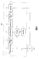
Figure 1 shows that the circuit structure diagram of radio wave clock 900.Radio wave clock 900 comprises: CPU (Central Processing Unit, CPU) 901, input unit 902, display unit 903, RAM (Random Access Memory, random access memory) 905, ROM (Read Only Memory, read-only memory) 906, receive control unit 907, timing circuit 908 and time code converting unit 910.Each unit connects by bus 913, and in addition, oscillating circuit 909 is connected to timing circuit 908.
Under the control of CPU 901, RAM 905 stores the data of being handled by CPU 901, and the data of storage are outputed to CPU 901.System program and application program that the main storage of ROM 906 and radio wave clock 900 are relevant.In addition, according to present embodiment, ROM906 storing frequencies conversion program 916.Frequency inverted program 916 is the programs that are used for controlling the frequency selective network 2 that comprises in the radio wave reception device 917 of waiting a moment description, to change selected frequency.
Receive control unit 907 and comprise that radio wave reception device 917. radio wave reception devices 917 remove the unwanted frequency composition from the standard radio wave that receives by antenna, picking out the target frequency signal, and will output to time code converting unit 910 from this frequency signal electrical signal converted.
Time code converting unit 910 is according to the signal from radio wave reception device 917 outputs, generation comprises the standard time code as the needed data of the function of clock (for example standard time code, total code, Zhou Lidai sign indicating number etc.), and the standard time code that produces is outputed to CPU 901.
Fig. 2 is the block diagram of demonstration according to the circuit structure of the radio wave reception device 917 of the employing superhet method of present embodiment.Radio wave reception device 917 comprises antenna 1, frequency selective network 2, radio-frequency amplifier circuit 3, freq converting circuit 4, local oscillation circuit 5, filter circuit 6, intermediate frequency amplifier circuit 7 and testing circuit 8.
Frequency selective network 2 receives from the signal of antenna 1 output, and selection and output frequency are the signal of f1 or f2, in the present embodiment, should select to have frequency be the signal of f1 as initial setting up frequency selective network 2 according to being f1 or f2 with frequency inverted to be selected from the signal S1 of testing circuit 8 inputs or from the signal S2 of CPU 901 inputs.
The signal that radio-frequency amplifier circuit 3 amplifies and output is imported from frequency selective network 2, antenna 1 and frequency selective network 2 all have the function of radio wave receiving system.
In addition, testing circuit 8 determines whether to have imported any signal from intermediate frequency amplifier circuit 7.For example, under the situation of the signal that frequency of antenna 1 reception is f2, because frequency selective network 2 by initial setting up, makes its selection have the signal of frequency f 1, so do not select to have the signal of frequency f 2.That is, because not from frequency selective network 2 output signals, so there is not signal to be input to testing circuit 8.Therefore, testing circuit 8 has determined whether that any signal is input to wherein, and will determine that the result outputs to frequency selective network 2 as signal S1.Based on this signal S1, frequency selective network 2 will treat that selected frequency is transformed into f2 from f1, perhaps be transformed into f1 from f2.Testing circuit 8 has the function of checkout gear.
Be output to time code converting unit 910 and be converted into the standard time code from the signal with frequency f d of testing circuit 8 outputs.This standard time code is imported into CPU901, and is used for various operations, for example revises current time data.If all in the zone that can receive two kinds of standard radio waves, be received with frequency f 1 and f2 owing to have two kinds of signals of frequency f 1 and f2 respectively, the signal that then initial setting up assigned frequency selects circuit 2 should select to have frequency f 1 outputs to radio-frequency amplifier circuit 3 so frequency selective network 2 will have the signal of frequency f 1.Yet,, will may not be converted to correct standard time code by time code converting unit 910 in some cases from the signal of testing circuit 8 outputs if the signal with frequency f 1 that is received is very weak.As a result, CPU 901 problem of executable operations has correctly appearred.
Therefore, in the timing of CPU 901 from time code converting unit 910 acceptance criteria time codes, CPU 901 starts the execution of frequency inverted program 916, and carries out frequency-conversion operation.Fig. 3 is the operational flowchart that shows radio wave clock 900 when carrying out frequency-conversion operation.At first, determine that at CPU 901 not free codes are not that (steps A 1: not), CPU901 outputs to frequency selective network 2 (steps A 2) with signal S2 under the situation of correct time code from 910 inputs of time code converting unit or input signal.Based on this signal S2, frequency selective network 2 will treat that selected frequency is transformed into f2 or is transformed into f1 from f2 from f1.That is, under the very weak situation of the signal with a kind of frequency, may make frequency selective network 2 select signal with another kind of frequency.
For intermediate frequency fi is fixed, use the radio wave reception device 917 of common superhet method to change local frequency according to the frequency that is input to the signal of freq converting circuit 4 usually.In this case, need to use PLL (Phase Locked Looop phase-locked loop) circuit to wait and change local frequency.Here the problem of Cun Zaiing is: circuit quantity has increased, and the circuit structure of radio wave reception device 917 becomes complicated.In addition, the increase of circuit quantity cause another problem the time power consumption also increased.
Therefore, now the method that local frequency f0 is set will be described, and, under the situation that does not change local frequency f0, intermediate frequency fi be remained unchanged after frequency inverted according to this method.
Fi=f1-f0---(1) or
fi=f2-f0---(2)
Set up.
With modulation comprises time code and has the low frequency standard radio wave of frequency f 1 or f2 as PWM (pulse-width modulation) method that shows among Figure 12, and transmit this low frequency standard radio wave with 100% and 10% the index of modulation.Then, from this radio wave, detect baseband signal.Because the frequency spectrum that sideband wave (respectively above and below carrier wave) expression is identical is so higher and lower sideband wave can exchange mutually.
Therefore, the fi in equation (1) and (2) can be write as
1/
2Fi
1/
2Then, the fi in supposition equation (2) is-situation of fi under, equation:
Fi=f1-f0---(1) or
-fi=f2-f0---(3)
Set up.If with equation (1) and equation (3) addition, it causes
0=f1+f2-2f0。
This equals
f0=(f1+f2)/2---(4)。
That is, if local frequency f0 is set at the mean value of frequency f 1 and f2, two kinds of frequencies then, just frequency f 1 and frequency f 2 can be received.
Since same as described above, do not need to consider putting upside down of higher and lower sideband wave, and f1 and f2 in equation (1) and the equation (3) can be write as
1/
2F1
1/
2With
1/
2F2
1/
2Then, if the f2 in the equation (3) is assumed that-f2 equation then:
Fi=f1-f0---(1) or
-fi=-f2-f0---(5)
Set up.If with equation (1) and equation (5) addition, it causes
0=f1-f2-2f0。
Thereby, equation
f0=(f1-f2)/2---(6)
Set up.Equally, if local frequency f0 is set at 1/2 (mean value of difference) of difference between frequency f 1 and the f2, two kinds of frequencies then, just frequency f 1 and frequency f 2 can be received.
For example, under the situation of frequency f 1=60kHz and frequency f 2=40kHz, equation (4) will for
f0=(60+40)/2=50[kHz]---(7),
And equation (6) will for
f0=(60-40)/2=10[kHz]---(8)。
Therefore, by local frequency f0 is set at 50kHz or 10kHz, when any one is imported into freq converting circuit 4 in the signal with frequency 40kHz and 60kHz, may export constant intermediate frequency fi.
Then, will explain frequency f 1 or f2 and the synthetic method of local frequency f0.Under the situation of setpoint frequency f1=60kHz, frequency f 2=40kHz and local frequency f0=10kHz, will from the frequency of the signal of freq converting circuit 4 output will for
F1+f0=60+10=70[kHz]---(a) or
f1-f0=60-10=50[kHz]---(b),
F2+f0=40+10=50[kHz]---(c) or
f2-f0=40-10=30[kHz]---(d)。
Therefore, if the setpoint frequency of filter circuit 6 is 50[kHz], then by equation (b) and (c) the synthetic signal of method of expression pass through filter circuit 6, be output to intermediate frequency amplifier circuit 7.On the other hand, by equation (a) and (d) the synthetic filtered device circuit 6 of signal of method of expression filter out.Amplified by intermediate frequency amplifier circuit 7 from the signal of filter circuit 6 outputs, and detect its baseband signal by testing circuit 8.
In addition, under the situation of setting local frequency f0=50kHz, will from the frequency of the signal of freq converting circuit 4 outputs will for
F1+f0=60+50=110[kHz]---(e) or
f1-f0=60-50=10[kHz]---(f),
F2+f0=40+50=90[kHz]---(g) or
f2-f0=40-50=-10[kHz]---(h)。
In this case, produce by synthesizing of signal owing to have the both positive and negative frequency of same absolute, so the value of equation (h) can be handled according to its absolute value.Therefore, if the setpoint frequency of filter circuit 6 is assumed that 10[kHz], by equation (f) and (h) the synthetic signal of the method for expression be output to intermediate frequency amplifier circuit 7 by filter circuit 6.On the other hand, by equation (e) and (g) the synthetic filtered device circuit 6 of signal of method of expression filter out.
Radio wave reception device 917 of the present invention is not limited to described so far example, but can carry out various modifications in the scope of meaning of the present invention.For example, receive two or more frequencies in order to make radio wave reception device 917, according to the frequency that frequency selective network 2 is selected, the local frequency that can double f0.
Just as described above, to fix by making local frequency f0, a radio wave reception device 917 can receive the radio wave of two kinds of frequencies.In addition, owing to no longer need PPL circuit etc. by local frequency f0 is fixed, thus can reduce the ratio of circuit, and simplify circuit.So, amount of power dissipation and cost can reduce.In addition, since the radio wave that will receive for having low-frequency radio wave, so can in chip, form radio wave reception device 917.If realized this technology, then can further reduce circuit area, and also can save cost.
Second embodiment
Then, will explain the second embodiment of the present invention.Except with the radio wave reception device 920 instead of wireless radio-wave receivers 917 shown in Figure 4, identical with the structure of radio wave clock 900 shown in Figure 1 according to the structure of the radio wave clock of second embodiment of the invention.Therefore, will represent identical structural detail with identical reference number, and will omit the explanation of these structural details.
Fig. 4 is the block diagram of demonstration according to the circuit structure of the radio wave reception device 920 of present embodiment.Sync detection circuit 10 uses the signal that has with the carrier wave same frequency, comes to detect baseband signal from the signal of intermediate frequency amplifier circuit 7 inputs, and is that the signal of fd outputs to time code converting unit 910 with frequency.Sync detection circuit 10 comprises an oscillating circuit 110, and it is the signal oscillating of f0 ' that this oscillating circuit 110 makes frequency.Detected by the radio wave that sync detection circuit 10 is used for carrying out by oscillating circuit 110 oscillatory signal, output to phase-shift circuit 11 then.Here, frequency f 0 '=relation of frequency f i sets up.
In addition, sync detection circuit 10 determines whether to have imported any signal from intermediate frequency amplifier circuit 7.Under the situation of the signal that frequency of antenna 1 reception is f2, be the signal of f1 because the initial setting up assigned frequency selects circuit 2 should select frequency, be the signal of f2 so frequency selective network 2 is not selected frequency.Therefore, sync detection circuit 10 has determined whether that any signal is input to it, and will determine that the result outputs to frequency selective network 2 as signal S3.Based on this signal S3, frequency selective network 2 will treat that selected frequency is transformed into f2 from f1, perhaps be transformed into f1 from f2.
Phase-shift circuit 11 is such circuit, promptly according to being input to the phase place of the signal of freq converting circuit 4, adjusts from the circuit of the phase deviation of the signal of oscillating circuit 110 inputs.
Then, with the relation of explaining between local frequency f0, intermediate frequency fi and the frequency dividing circuit 12.Radio wave reception device 920 promptly satisfies equation (4) or (6) based on following hypothesis in the middle of local frequency f0, frequency f 1 and frequency f 2, so that can receive the signal of two kinds of frequencies, that is, and frequency f 1 and frequency f 2.Therefore, under the situation of supposition local frequency f0 by equation (4) expression, equation
Fi=f1-f0[is from equation (1)]
=f1-{(f1+f2)/2}
=(f1-f2)/2---(9)
Set up.In addition, under the situation of supposition local frequency f0 by equation (6) expression, equation
fi=f1-f0
=f1-{(f1-f2)/2}
=(f1+f2)/2---(10)
Set up.
Under the situation of supposition frequency f 1=60kHz, frequency f 2=40kHz and local frequency f0=10kHz, from the frequency of the signal of freq converting circuit 4 outputs will for
F1+f0=60+10=70[kHz]---(i) or
f1-f0=60-10=50[kHz]---(j),
F2+f0=40+10=50[kHz]---(k) or
f2-f0=40-10=30[kHz]---(m)。
Thereby, if the setpoint frequency of filter circuit 6 is 50[kHz], by equation (j) and (k) signal flow that synthesizes of method of expression be output to intermediate frequency amplifier circuit 7 then through filter circuit 6.
Detect owing to carry out radio wave, so must satisfy equation f0 '=fi=50kHz by synchronization detecting method.Therefore, if frequency dividing circuit 12 utilize 5 come to frequency f 0 '=signal of 50kHz carries out frequency division, when obtaining the concerning of f0=10kHz, then can produce the signal that local frequency is f0, makes it possible to receive the radio of two kinds of frequencies.
Under the situation of supposition local frequency f0=50kHz, will from the frequency of the signal of freq converting circuit 4 outputs will for
F1+f0=60+50=110[kHz]---(n) or
f1-f0=60-50=10[kHz]---(o),
F2+f0=40+50=90[kHz]---(p) or
f2-f0=40-50=-10[kHz]---(q)。
In this case, because synthesizing by signal, two positive and negative frequencies with same absolute produce, so the value of equation (q) can be handled according to its absolute value.Therefore, if the setpoint frequency of filter circuit 6 is assumed to 10[kHz], then the signal flow that synthesizes by equation (o) and the method (q) represented is through filter circuit 6, and is output to intermediate frequency amplifier circuit 7.
In this case, if replace frequency dividing circuit 12 with multiple circuit, and this multiple circuit with frequency f 0 ' (=fi)=signal times of 10kHz is with 5, and obtain the relation of f0=50kHz, then can produce the signal that local frequency is f0, make it possible to receive the radio wave of two kinds of frequencies.
Just as described above, carry out frequency division or the multiplication computing produces the signal that local frequency is f0 by signal to 110 outputs of the oscillating circuit that from sync detection circuit 10, comprises, do not need to be provided for separately exporting the oscillating circuit that local frequency is the signal of f0.Therefore, can dwindle circuit size, simplify the structure of circuit and also reduced power consumption.Phase-shift circuit 11 can be arranged on sync detection circuit 10 inside.
The 3rd embodiment
In a second embodiment, produce the signal of local frequency by the oscillating circuit 110 that uses sync detection circuit 10 as f0.In the present embodiment, will explain radio wave reception device 930, radio wave reception device 930 uses from the signal of local oscillation circuit 5 outputs, and the radio wave that this signal is used for being undertaken by sync detection circuit 10 detects.Except with the radio wave reception device 930 instead of wireless radio-wave receivers 917 shown in Figure 5, identical with the structure of radio wave clock 900 shown in Figure 1 according to the structure of the radio wave clock of the 3rd embodiment.Therefore, will represent identical structural detail, and omit explanation these structural details with identical reference number.
Fig. 5 is the block diagram of demonstration according to the circuit structure of the radio wave reception device 930 of present embodiment.Sync detection circuit 40 comprises local oscillation circuit 5, multiple circuit 13 and sync detection circuit 14.It is the signal of f0 that multiple circuit 13 receives local frequency from local oscillation circuit 5, and this signal that doubles.Then, multiple circuit 13 is that the signal of f0 ' outputs to sync detection circuit 14 with frequency multiplication.
Then, will explain local frequency f0, intermediate frequency fi, and the relation of multiple circuit 13.Radio wave reception device 930 promptly between local frequency f0, frequency f 1 and frequency f 2, satisfies equation (4) or (6) represented relation based on following hypothesis, so that can receive the radio wave of f1 and two kinds of frequencies of f2.Thereby, in the situation of supposition local frequency f0 by equation (4) expression, equation
Fi=f1-f0[is from equation (1)]
=f1-{(f1+f2)/2}
=(f1-f2)/2---(11)
Set up.In the situation of supposition local frequency f0 by equation (6) expression, equation
fi=f1-f0
=f1-{(f1-f2)/2}
=(f1+f2)/2---(12)
Set up.
In the situation of supposition frequency f 1=60kHz, frequency f 2=40kHz and local frequency f0=10kHz, will from the frequency of the signal of freq converting circuit 4 outputs will for
F1+f0=60+10=70[kHz]---(r) or
f1-f0=60-10=50[kHz]---(s),
F2+f0=40+10=50[kHz]---(t) or
f2-f0=40-10=30[kHz]---(u)。
Thereby, if the setpoint frequency of filter circuit 6 is assumed to 50[kHz], then by equation (s) and the signal flow that synthesizes of the method for (t) representing through filter circuit 6, and be output to intermediate frequency amplifier circuit 7.
Owing to be input to the frequency f 0 of the signal of sync detection circuit 14 ' need be identical, so must satisfy equation f0 '=fi=50kHz with the frequency (for example, intermediate frequency fi) of carrier wave.Therefore, multiple circuit 13 with 5, and obtains the relation of f0 '=50kHz with the signal times of local frequency f0=10kHz.Then, multiple circuit 13 outputs to sync detection circuit 14 with the signal of multiplication.
In addition, at supposition local frequency f0=50[kHz] situation in, will from the frequency of the signal of freq converting circuit 4 outputs will for
F1+f0=60+50=110[kHz]---(v) or
f1-f0=60-50=10[kHz]---(w),
F2+f0=40+50=90[kHz]---(x) or
f2-f0=40-50=-10[kHz]---(y)。
In this case, synthesize by signal and produce positive and negative two frequencies with same absolute.Therefore, the value of equation (y) can be handled according to its absolute value.Thereby, if the setpoint frequency of filter circuit 6 is assumed to 10[kHz], so by equation (w) and (y) signal flow that synthesizes of method of expression and be output to intermediate frequency amplifier circuit 7 through filter circuit 6.
In this case, if replace multiple circuit 13 with frequency dividing circuit, then this frequency dividing circuit utilizes the signal of 5 couples of frequency f 0=50kHz to carry out frequency division, and can obtain f0 '=10kHz.Because frequency f 0 ' consistent, so can carry out synchronous detecting with intermediate frequency fi.
Just as described above, by the signal from local oscillation circuit 5 output being carried out frequency division or sync detection circuit 14 is operated in multiplication, do not need oscillating circuit to be set to sync detection circuit 14.Therefore, can reduce the size of circuit, and the structure of simplifying circuit.And because oscillating circuit is used jointly, so also reduced power consumption.
The 4th embodiment
Then, will explain the fourth embodiment of the present invention.Except replacing the radio wave reception device 917 shown in Figure 1, identical with the structure of radio wave clock 900 shown in Figure 1 according to the structure of the radio wave clock of the 4th embodiment with radio wave reception device 940 shown in Figure 6 or radio wave reception device shown in Figure 8 950.Therefore, will represent identical structural detail, and omit explanation these structural details with identical reference number.
In addition, in the present embodiment, will explain that as an example radio wave reception device of the present invention is used for the situation of radio wave clock.Yet the present invention is not limited to radio wave reception device, but can adopt any equipment that is used to receive radio wave.
Fig. 6 is the block diagram of demonstration according to the circuit structure of the radio wave reception device 940 of the employing superhet method of present embodiment.Radio wave reception device 940 comprises: antenna 1, frequency selective network 2, radio-frequency amplifier circuit 3, frequency translation circuit 4, local oscillation circuit 5, filter circuit 6, intermediate frequency amplifier circuit 7, testing circuit 8 and multiple circuit 9.
Frequency selective network 2 receives from the signal of antenna 1 output, and select and output frequency be f1 or f2 signal in the present embodiment, be that the signal of f1 is as initial setting up selecting frequency.According to the signal S2 by CPU 901 inputs, frequency selective network 2 is f1 or f2 with frequency inverted to be selected.Antenna 1 and frequency selective network 2 all have the function as the radio wave receiving system.
Radio-frequency amplifier circuit 3 amplifies from the signal of frequency selective network 2 inputs, exports amplifying signal then.Freq converting circuit 4 will be synthetic with the signal of importing from multiple circuit 9 from the signal of radio-frequency amplifier circuit 3 inputs, and the output intermediate frequency is the signal of fi.Freq converting circuit 4 has the function as frequency conversion apparatus.
It is the signal of f0 that local oscillation circuit 5 produces local frequency, and this signal is outputed to multiple circuit 9.Local oscillation circuit 5 has the function of oscillation device.After a while the method that local frequency f0 is set will be described.In addition, local oscillation circuit 5 comprises having the circuit (not shown) of determining the function of device as frequency.
In addition, testing circuit 8 determines whether to have imported any signal from intermediate frequency amplifier circuit 7.For example, if the signal that it is f2 that antenna 1 receives a frequency because initial setting frequency selective network 2 should to select frequency be the signal of f1, be the signal of f2 so frequency selective network 2 is not selected frequency.That is, because not from frequency selective network 2 output signals, so cause do not have signal to be input to the problem of testing circuit 8.Therefore, testing circuit 8 has determined whether that any signal is input to testing circuit 8, and will determine that the result outputs to CPU 901 as signal S1.Based on this signal S1, frequency selective network 2 will treat that selected frequency is transformed into f2 or is transformed into f1 from f2 from f1, and multiple circuit 9 is converted to stand-by multiplication value from the signal of local oscillation circuit 5 inputs.
From the frequency of testing circuit 8 output is that the signal of fd is output to time code converting unit 910, and converts the standard time code to.This standard time code is imported into CPU901, and is used for various operations, for example revises current time data.For example, in frequency is that two kinds of standard radio waves of f1 and f2 can both received zone, antenna 1 receive frequency is respectively in the situation of signal of f1 and f2, to select frequency be the signal of f1 because frequency selective network 2 is initially set to, so frequency selective network 2 is that the signal of f1 outputs to radio-frequency amplifier circuit 3 with frequency.Yet, be weak if the frequency that receives is the signal of f1, some situation, may not be converted to correct standard time code from the signal of testing circuit 8 outputs by time code converting unit 910.As a result, the problem of generation is that CPU 901 can not correctly carry out various operations.
For addressing the above problem, CPU 901 begins to carry out changeover program 916 in the predetermined timing of setting in advance, and carries out and cut conversion operations.Fig. 7 is the schematic diagram that shows the operating process of radio wave clock 900 when conversion operations is cut in execution.At first, CPU 901 determines whether to have imported signal S1 (steps A 1) from testing circuit 8.Signal S1 is such signal, and promptly when not having signal when intermediate frequency amplifier circuit 7 is input to testing circuit 8, testing circuit 8 outputs to the signal of CPU 901.Be imported in the situation of CPU 901 (steps A 1: be) at signal S1, CPU 901 is advanced to steps A 3 with flow process.
(steps A 1: not), CPU901 does not determine whether from the signal of time code converting unit 910 outputs be correct standard time code (steps A 2) in signal S1 is imported into the situation of CPU 901.Determine under the situation of the correct standard time code of time code converting unit 910 outputs (steps A 2: be), CPU 901 terminating operations at CPU.On the other hand, determine that at CPU correct standard time code is not that (steps A 2: not), CPU 901 outputs to frequency selective network 2 and multiple circuit 9 (steps A 3) with signal S2 under the situation of time code converting unit 910 outputs.Based on signal S2, frequency selective network 2 will treat that selected frequency switches to f2 or switches to f1 from f2 from f1.Based on signal S2, multiple circuit 9 switches to local frequency f0 with stand-by multiplication value.Therefore, if it is very weak to have a kind of signal of frequency, can make frequency selective network 2 select signal with another kind of frequency.
The radio wave reception device that uses superhet method commonly used usually according to be input to freq converting circuit the frequency of signal change local frequency.So that intermediate frequency fi is fixed.In this case, be necessary to use PLL (Phase Locked Loop phase-locked loop) circuit to wait and change local frequency.Here the problem of Cun Zaiing is: circuit quantity increases, and the circuit structure of radio wave reception device becomes complicated.In addition, another problem of causing of the increase of circuit quantity is: power consumption also increases.
Therefore, will explain the method for setting local frequency f0 now.According to this method, it is constant that intermediate frequency fi is continued after frequency inverted, and do not change local frequency f0.
Utilize fixedly local frequency f0, the purpose of freq converting circuit 4 is: the frequency that receives by synthetic antenna 1 is that the signal of f1 is the signal of nf0 with by multiple circuit 9 local frequency f0 being multiply by the frequency that n obtains, and to export intermediate frequency be the signal of fi and make.In addition, the purpose of freq converting circuit 4 is: the signal that by frequency synthesis is f2 is the signal of mf0 with by multiple circuit 9 local frequency f0 being multiply by the frequency that m obtains, and is the signal of fi and make the output intermediate frequency.PWM (Pulse Width Modulation pulse-width modulation) method modulation by showing among Figure 12 comprises time code and frequency is the radio wave of the low frequency standard of f1 or f2, and transmits with 100% and 10% modulation factor.From this radio wave, detect baseband signal.Because the frequency spectrum that sideband wave (respectively above and below carrier wave) expression is identical is so high and low sideband wave can exchange mutually.Therefore, equation
Fi=|f1 ± nf0| or fi=|f2 ± mf0|---(1 ')
Can set up.
According to equation (1 '), below four groups of equatioies all set up:
Fi=f1+nf0 or fi=f2+mf0---(2 ')
Fi=f1+nf0 or fi=|f2-mf0|---(3 ')
Fi=f1-nf0 or fi=f2+mf0---(4 ')
Fi=f1-nf0 or fi=|f2-mf0|---(5 ')
Therefore, according to equation (2 '), following equation is set up:
f1+nf0=f2+mf0
f1-f2=(m-n)f0
f0=(f1-f2)/(m-n) ---(6’)
Equally, according to equation (3 '), following equation is set up:
f1+nf0=|f2-mf0|
f1+nf0=f2-mf0
f1-f2=-(m+n)f0
f0=(f1-f2)/{-(m+n)}---(7’)
Or
f1+nf0=-(f2-mf0)
f1+f2=(m-n)f0
f0=(f1+f2)/(m-n)---(8’)
Equally, according to equation (5 '), following equation is set up:
|f1-nf0|=|f2-mf0|
f1-nf0=f2-mf0
f1-f2=-(m-n)f0
f0=(f1-f2)/{-(m+n)}---(9’)
Or
f1-nf0=-(f2-mf0)
f1+f2=(m+n)f0
f0=(f1+f2)/(m+n)---(10’)
Because the equation that obtains by extended equation (4 ') is equivalent to equation (7 ') and equation (8 '), so omitted the expansion of equation (4 ').In addition, equation (6 ') and equation (9 ') equivalent equivalence.Thereby, can be 40[kHz as f1 in equation (7 ') to (10 ') by alternative] and f2 be 60[kHz], calculate local frequency f0.In the situation of supposition n=1 and m=2, obtain from equation (7 '):
f0=6.666[kHz]---(11’)。
Equally, obtain from equation (8):
f0=100[kHz]---(12’)。
Obtain from equation (9 '):
f0=20[kHz]---(13’)。
Obtain from equation (10 '):
f0=33.333[kHz]---(14’)。
By as described above, setting local frequency f0, as frequency f 1=40[kHz] signal and frequency f 2=60[kHz] signal in any one signal when being imported into freq converting circuit 4, can export sustained intermediate frequency fi.
Then, with the method for explaining that frequency f 1 or f2 and local frequency are synthetic.For example, suppose f1=40[kHz], f2=60[kHz], and the local frequency f0=100[kHz of equation (12 ')].At n=1, in the situation of m=2, from the intermediate frequency fi of the signal of freq converting circuit 4 output will for
F1+nf0=40+100=140[kHz]---(a ') or
| f1-nf0|=|40-100|=60[kHz]---(b ') or
F2+mf0=60+2 * 100=260[kHz]---(c ') or
|f2-mf0|=|60-2×100|=140[kHz]---(d’)。
In this case, if the setpoint frequency of supposition filter circuit 6 is 140[kHz], then the signal flow that synthesizes of the method for representing by equation (a ') and (d ') is through filter circuit 6, and is output to intermediate frequency amplifier circuit 7.On the other hand, the filtered device circuit 6 of signal that synthesizes by equation (b ') and (c ') method of expression filters.
For example, suppose the multiple circuit setting that is initialised, make it will output to freq converting circuit 4, and local frequency f0 is not processed at the local frequency f0 of this input.Then, if antenna receives frequency f 1=40[kHz] signal, then freq converting circuit 4 is with frequency f 1=40[kHz] signal and the frequency signal that is f0 synthesize, this be because, as mentioned above, frequency selective network 2 setting that is initialised, making it should select frequency is the signal of f1.Then, have only the signal that synthesize by the method for equation (a ') expression to pass through filter circuit 6, and be output to intermediate frequency amplifier circuit 7.
On the other hand, if antenna 1 receives frequency f 2=60[kHz] radio wave signal, then as mentioned above, CPU 901 output signal S2, and frequency selective network 2 will treat that selected frequency switches to f2 from f1.In addition, multiple circuit 9 switches setting according to signal S2, and it should be exported the signal times that inputs to it with 2.Thereby, frequency f 2=60[kHz] signal and frequency 2f0=200[kHz] signal will be synthetic by freq converting circuit 4.Then, have only the signal that synthesize by the method for equation (d ') expression to pass through filter circuit 6, and be output to intermediate frequency amplifier circuit 7.
Equally, suppose f1=40[kHz], f2=60[kHz], and from the local frequency f0=100[kHz of equation (12 ')].Then, under the situation of supposition n=2 and m=1, will from the intermediate frequency fi of the signal of freq converting circuit 4 outputs will for:
F1+nf0=40+2 * 100=240[kHz]---(e ') or
| f1-nf0|=|40-2 * 100|=160[kHz]---(f ') or
F2+mf0=60+100=160[kHz]---(g ') or
|f2-mf0|=|60-100|=40[kHz]---(h’)。
In this case, if the setpoint frequency of supposition filter circuit 6 is 160[kHz], then the signal that synthesizes by equation (f ') and (g ') method of expression passes through filter circuit 6, and is output to intermediate frequency amplifier circuit 7.On the other hand, the filtered device circuit 6 of signal that synthesizes by equation (e ') and (h ') method of expression filters.
Equally, for by equation (11 '), (13 ') and (14 ') represented local frequency f0, by supposition f1=40[kHz] and f2=60[kHz] intermediate frequency fi calculated.Obtain following result:
At f0=6.666[kHz] situation under (11 ')
In the situation of n=1 and m=2, fi=46.666[kHz], or
In the situation of n=2 and m=1, fi=53.333[kHz]
At f0=20[kHz] situation under (13 ')
In the situation of n=1 and m=2, fi=20[kHz], or
In the situation of n=2 and m=1, fi=80[kHz]
At f0=33.333[kHz] situation in down (11 ')
In the situation of n=1 and m=2, fi=6.666[kHz], or
In the situation of n=2 and m=1, fi=26.666[kHz]
Thereby, for each local frequency f0, can export sustained intermediate frequency fi.Realization degree of the filter function of the reception by considering interference, picture frequency to fundametal compoment and harmonic component, noise conditions, filter circuit 6 or the like will be identified for the combination of the local frequency f0 and the intermediate frequency fi of radio wave reception device 914.
According to the frequency of the signal that will be input to freq converting circuit 4, by select from the local frequency f0 of local oscillation circuit 5 outputs the n level (for example elementary, secondary ...) harmonic component, make and can export intermediate frequency fi.This method can realize by radio wave reception device 950 shown in Figure 8.Difference between radio wave reception device 940 shown in Figure 6 and the radio wave reception device 950 is whether have multiple circuit 9.That is in radio wave reception device 950, be that the signal of f0 is output to freq converting circuit 4, from the local frequency of local oscillation circuit 5 output.Then, freq converting circuit 4 is the harmonic component of the signal of f0 according to selecting local frequency from the frequency of the signal of sending out radio-frequency amplifier circuit 3 inputs.Then, freq converting circuit 4 by with local frequency be f0 signal selection harmonic component with synthesize from the signal of sending out radio-frequency amplifier circuit 3 inputs, export the signal that intermediate frequency is sustained fi.In this case, because do not need to be provided with multiple circuit, thus can reduce the area of entire circuit, and reduce power consumption.
As described till now, can be by local frequency f0 fixedly being received the radio wave of two kinds of frequencies.In addition, because pass through fixedly local frequency f0, making does not need to be provided with the PLL circuit, thus can reduce circuit scale, and simplify circuit structure.Therefore, can reduce power consumption and cost.In addition, because the radio wave that receives is a low frequency radio wave, so can in chip, form radio wave reception device 940 or radio wave reception device 950.If realize above-mentioned setting, then can further reduce circuit area, and also can reduce cost.
The 5th embodiment
Then, will explain the fifth embodiment of the present invention.Except replaced CPU 901 shown in Figure 1 with CPU 9010, and replaced outside the radio wave reception device 917 shown in Figure 1 with radio wave reception device 960 shown in Figure 9 or radio wave reception device shown in Figure 11 970, identical according to the structure of the radio wave clock of the 5th embodiment with the structure of radio wave clock 900 shown in Figure 1.Therefore, will represent identical structural detail, and omit explanation these structural details with identical reference number.
In addition, in the present embodiment, the situation when explaining that as an example radio wave reception device of the present invention is used for radio wave clock.Yet the present invention is not limited to radio wave reception device, but can adopt the equipment of any reception radio wave.
In the 4th embodiment, the radio wave reception device 940 and the radio wave reception device 950 that can receive two kinds of frequencies (40[kHz just] and 60[kHz]) radio wave have been explained.In the present embodiment, will explain radio wave reception device 960 and radio wave reception device 970, wherein in local frequency fixedly the time, radio wave reception device 960 and radio wave reception device 970 can receive the radio wave of three kinds of frequencies.
Fig. 9 is the block diagram of demonstration according to the circuit structure of the radio wave reception device 960 of present embodiment.CPU 9010 receives from the identification signal of the inputs such as switch that constitute input unit 902.This identification signal is the signal that for example is used to indicate the country that uses radio wave.
Then, will explain the method for setting wireless radio-wave receiver 960 employed local frequency f0, it is constant wherein according to this local frequency f0 the intermediate frequency fi that obtains after frequency inverted to be continued, and there is no need to change local frequency f0 simultaneously.In the number of frequencies that antenna 1 is received is two or more situation, by obtaining to satisfy the local frequency f0 of the represented relation of equation (15), can export lasting constant intermediate frequency fi, wherein equation (15) arrives (5 ') based on above-mentioned equation (1 ').
(|f1±fi|/p1)=...=(|fn±fi|/pn)=f0(15)
At this, n is equal to or greater than 2 integer, and p1 ..., pn is positive integer.Present embodiment relates to the radio wave reception device that can receive three kinds of frequency wireless electric waves.Therefore, should obtain to satisfy the local frequency f0 and the intermediate frequency fi of following equation (16).
(|f1±fi|/p1)=(|f2±fi|/p2)=(|f3±fi|/p3)=f0---(16)
Particularly, by using 40[kHz] replace f1, use 60[kHz] replace f2, and use 77.5[kHz] (frequency that comprises the low frequency standard radio wave of time code in Germany) replacement f3, equation (16) will for
(|40±fi|/p1)=(|60±fi|/p2)=(|77.5±fi|/p3)(17)
By using equation (17), with the value that obtains to make p1, p2, p3 value for the intermediate frequency fi of positive integer, for example, if suppose fi=22.5[kHz], equation (17) will for
(|40±22.5|/p1)=(|60±22.5|/p2)=(|77.5±22.5|/p3)(18)
In addition, if any one makes equation (18) satisfy in plus sige in the molecule and the minus sign, its result is
(62.5/p1)=(37.5/p2)=(100/p3)(19)
Therefore, if suppose p1=5, p2=3, p3=8, then local frequency f0 will be 12.5[kHz].That is, at f1=40[kHz], f2=60[kHz] and f3=77.5[kHz] situation under, by with local frequency f0 stuck-at-2.5[kHz], and carry out following calculating, export sustained intermediate frequency fi=22.5[kHz].
-be that the signal of f1 is imported in the situation of freq converting circuit in frequency, local frequency f0 should multiply by 5.
-be that the signal of f2 is imported in the situation of freq converting circuit in frequency, local frequency f0 should multiply by 3.
-be that the signal of f3 is imported in the situation of freq converting circuit in frequency, local frequency f0 should multiply by 8.
Then, the operation that connects clock according to the radio wave of present embodiment will be explained.For example, suppose three kinds of frequencies (just, the Japanese frequency f 1=40[kHz that comprises the low frequency standard radio wave of time code] and f2=60[kHz], and the German frequency f 3=77.5[kHz that comprises the low frequency standard radio wave of time code]) can both be received.In addition, suppose that frequency selective network 2 is initially set that to select frequency be the signal of f1, and multiple circuit is set to and local frequency f0 be multiply by 5 exports.
Receive signal that frequency is f2 or time code converting unit 910 is not exported correct standard time code or under the situation of input unit 902 input identifying informations (expression uses the country of radio wave to forward Germany to from Japan) at antenna 1, need to switch the frequency that to be selected by frequency selective network 2 and the multiplication value that will be used for local frequency f0 by multiple circuit 9.
Therefore, CPU 9010 begins to carry out the frequency changeover program in predetermined timing, wherein should predetermined timing be set in advance, so that carry out handover operation.Figure 10 is the schematic diagram that shows when the operating process of the radio wave clock of execution during according to the frequency handover operation of present embodiment.At first, CPU 9010 determines whether from testing circuit 8 input signal S1 (step B1).Be imported at signal S1 under the situation of CPU 9010 (step B1: be), CPU 9010 is advanced to step B4 with flow process.
(step B1: not), CPU 9010 does not determine whether from the signals of time code converting unit 910 outputs be correct standard time code (step B2) in signal S1 is imported into the situation of CPU 9010.Do not export in time code converting unit 910 that (step B2: not), CPU 9010 is advanced to step B4 with flow process under the situation of correct standard time code.
On the other hand, under the situation of the correct standard time code of time code converting unit 910 output (step B2: be), CPU 9010 determine whether an identifying information be transfused to it (step B3).In the situation that does not have identifying information to be transfused to (step B3: not), CPU 9010 terminating operations.On the other hand, be imported in the situation of CPU 9010 (step B3: be) at identifying information, CPU 9010 outputs to frequency selective network 2 and multiple circuit 9 (step B3) with signal S3.Then, CPU 9010 terminating operations.
Just as described above, according to CPU 9010 output signal S3, frequency selective network 2 is the select target frequency from frequency f 1, f2, f3.In addition, multiple circuit 9 selects to be used for the multiplication value of local frequency based on signal S3.As a kind of system of selection, can comprise the pulse mode that combines with frequency f 1, f2 or f3 among the signal S3.Make and determine frequency to be selected and multiplication value according to each pulse mode.
Then, the operation of radio wave reception device 960 will be explained.Same as described above, suppose that radio wave reception device 960 can receive the signal of three kinds of frequencies, f1=40[kHz just], f2=60[kHz] and f3=77.5[kHz], and local frequency f0 is 12.5[kHz], with intermediate frequency fi=22.5[kHz], if antenna 1 receive frequency f1=40[kHz] signal, to select frequency be the signal of f1 because freq converting circuit 2 is initially set, so freq converting circuit 4 is with frequency f 1=40[kHz] signal be 62.5[kHz by local frequency f0 being multiply by 5 frequencies that obtain] signal synthesize.Then, having only the frequency as synthetic result's output is 22.5[kHz] signal by filter circuit 6, and be output to IF power amplifier circuit 7.
On the other hand, receive frequency f 2=60[kHz at antenna 1] the situation of radio wave under select frequency f 1=40[kHz because freq converting circuit 2 is initially set] signal, so there is not signal to output to testing circuit 8.Thereby testing circuit 8 outputs to CPU 9010 with signal S1.In view of the above, CPU 9010 is as above-mentioned output signal S3, and will treat that selected frequency switches to f2 from f1.In addition, according to signal S3, multiple circuit 9 switches setting, makes it that local frequency be multiply by 3 outputs.Thereby freq converting circuit 4 is with frequency f 2=60[kHz] signal and frequency be 37.5[kHz] signal synthesize.Then, having only frequency is 22.5[kHz] signal by ripple device circuit 6, and be output to IF power amplifier circuit 7.
In addition, be imported into the situation of CPU9010 in the identification signal that is used for indicating the country that uses radio wave, just as described above, CPU 9010 output signal S3.In response to S3, frequency selective network 2 will treat that selected frequency is transformed into f3 from f1 or f2.And multiple circuit 9 switches setting, makes it that local frequency be multiply by 8 outputs.Thereby freq converting circuit 4 is with frequency f 3=77.5[kHz] signal and frequency be 100[kHz] signal synthesize.Then, having only frequency is 22.5[kHz] signal by filter circuit 6, and be output to IF power amplifier circuit 7.
Just as described above, make them satisfy equation (15) by setting local frequency f0 and intermediate frequency fi, just can realize receiving the radio wave reception device of three kinds of frequencies.And, although explained the radio wave reception device that can receive three kinds of frequencies in the present embodiment, utilize equation (15) can realize receiving the radio wave reception device of four kinds or multiple frequency wireless electric wave.
According to the frequency of the signal that is input to freq converting circuit 4, by select from the local frequency f0 of local oscillation circuit 5 outputs the n level (for example elementary, secondary ...) harmonic component, make and can export intermediate frequency fi.This method can realize by radio wave reception device 970 shown in Figure 11.Difference between radio wave reception device 960 shown in Figure 9 and the radio wave reception device 970 is whether have multiple circuit 9.That is in radio wave reception device 960, be that the signal of f0 is output to freq converting circuit 4, from the local frequency of local oscillation circuit 5 output.Then, freq converting circuit 4 is the harmonic component of the signal of f0 according to selecting local frequency from the frequency of the signal of sending out radio-frequency amplifier circuit 3 inputs.Freq converting circuit 4 with local frequency be f0 signal selection harmonic component with synthesize from the signal of sending out radio-frequency amplifier circuit 3 inputs, the output intermediate frequency is the sustained signal of fi.In this case, because do not need to be provided with multiple circuit, thus can dwindle the area of entire circuit, and reduce power consumption.
Just as described above, by setting local frequency f0 and intermediate frequency fi, make radio wave reception device can when local frequency f0 and intermediate frequency fi are fixing, receive three kinds or multiple frequency based on equation (15).In addition, fix by making local frequency f0, PPL circuit etc. becomes and does not need.Therefore, can dwindle the circuit ratio, and simplify circuit connection structure.Meanwhile, can reduce power consumption and cost.In addition, because the wireless wave that receives is the low frequency wireless wave, so radio wave reception device 960 or radio wave reception device 970 can be set in chip.If realize above-mentioned setting, then can further dwindle circuit area, and also can reduce cost.
By adopting five embodiment to explain the present invention.Yet the present invention is not limited to above-mentioned five embodiment, but can carry out various modifications in the scope of the inventive method.For example, the 4th embodiment and the 5th embodiment have described CPU output signal S2 and signal S3.Replace, when from testing circuit 8 input signal S1, can construct a simple logic circuit that uses circuits for triggering, flip-flop circuit output signal S2 and signal S3.
According to the present invention, by the average of the frequency setting of the signal that will be exported by oscillation device for first and second radio wave frequency, perhaps be set at the average of the difference between them, when receiving radio wave with different frequency, can the sustained intermediate-freuqncy signal of output frequency, and do not have to change signal from oscillation device output.
So just eliminated the needs to complicated circuit, this complicated circuit is used for changing according to the radio wave frequency that receives the frequency of the signal of oscillation device output.That is, become complicated, and, can reduce the area and the cost of circuit by reducing the quantity of circuit by preventing circuit.
Even receive the radio wave with different frequency, by local frequency being set at frequency f 10, f0 obtains from following equation:
(| f1 ± fi|/p1)=...=(| fn ± fi|/pn)=f0 (p1 ..., pn is positive integer)
Wherein this equation defined a plurality of each frequencies that receive radio wave (f1 ..., fn (n is equal to or greater than 2 integer)) and intermediate frequency fi between relation, radio wave reception device can receive the radio wave of two or more frequencies at local frequency f0 and intermediate frequency fi fixedly the time.
In addition, in the radio wave reception device that can receive a plurality of frequencies, when local frequency f0 is fixed, increase output afterwards, can determine intermediate frequency fi by local frequency f0 is added.Therefore, do not need to be provided with complicated circuit, this complicated circuit is used for changing according to the radio wave frequency that receives the frequency of the signal of oscillation device output.That is, become complicated, and, can reduce the area and the cost of circuit by reducing the quantity of circuit by preventing circuit.
In addition, even receive radio wave, can produce the sustained intermediate-freuqncy signal of frequency by the harmonic component of the signal of the fixed frequency of oscillation device output and the signal of reception are synthesized with different frequency.Therefore, do not need to be provided with complicated circuit, this complicated circuit is selected the harmonic component of the signal of oscillation device output according to the radio wave frequency that receives, so that export intermediate frequency.That is, become complicated, and, can reduce the area and the cost of circuit by reducing the quantity of circuit by preventing circuit.
Various embodiment and modification be can construct here, and broad spirit of the present invention and scope do not deviated from.The foregoing description intention is to describe the present invention, rather than limits the scope of the invention.Scope of the present invention illustrates by additional claim, rather than embodiment.In the equivalent method scope of claim of the present invention and the modification of in the claim scope, being done all be considered within the scope of the invention.
The application is based on the Japanese patent application Nos.2002-233512 of submission on 08 09th, 2002 and the No.2002-245460 that submitted on 08 26th, 2002.The content of above-mentioned Japanese Patent Application Publication is herein incorporated by reference.
Claims (6)
1. radio wave reception device comprises:
Radio wave receiving system (1,2) receives radio wave signal, converts the radio wave signal that is received to the signal of telecommunication, and exports this signal of telecommunication;
Output has the oscillation device (5) of the signal of single-frequency;
Signal from described oscillation device (5) output is carried out the multiplying assembly (9) of frequency multiplication;
Frequency conversion apparatus (4) will synthesize with the signal of exporting from described multiplying assembly (9) from the signal of telecommunication of described radio wave receiving system (1,2) output, and the output intermediate-freuqncy signal; With
Checkout gear (8), the intermediate-freuqncy signal that demodulation is exported from described frequency conversion apparatus (4),
Wherein, described frequency conversion apparatus (4) will be synthesized with the signal of exporting from described multiplying assembly (9) by a signal in the signal with different frequency of described radio wave receiving system (1,2) reception, and export the intermediate-freuqncy signal that its frequency is fixed, wherein said single-frequency is to come well-determined by the described different frequency that uses the signal that is received by described radio wave receiving system (1,2).
2. according to the radio wave reception device of claim 1, wherein said oscillation device (5) comprises and is used for determining that the frequency of frequency f 0 determines device that this frequency f 0 obtains by following equation:
| f1 ± fi|/p1=...=|fn ± fi|/pn=f0, wherein p1 ..., pn is positive integer, a plurality of frequency f 1 of a plurality of radio waves that the definition of this equation is received by described radio wave receiving system (1,2) ..., the relation between the intermediate frequency fi of fn and single-frequency, wherein n is equal to or greater than 2 integer.
3. according to the radio wave reception device of claim 2, also comprise the choice device (901) that is used for selecting any one integer from positive integer p1 to pn,
Wherein, described multiplying assembly is exported this signal by multiply by the integer of being selected by described choice device (901) from the frequency of the signal with single-frequency of described oscillation device (5) output.
4. radio wave reception device comprises:
Radio wave receiving system (1,2) receives a plurality of radio waves with different frequency, and converts the signal of telecommunication to by each radio wave that will be received and export each the signal of telecommunication in these a plurality of radio waves;
Output has the oscillation device (5) of the signal of frequency f 0, and this frequency f 0 obtains by following equation:
| f1 ± fi|/p1=...=|fn ± fi|/pn=f0, wherein p1 ..., pn is positive integer, this equation defined a plurality of radio waves that can receive by described radio wave receiving system (1,2) each frequency f 1 ..., the relation between fn and the intermediate frequency fi, wherein n is equal to or greater than 2 integer;
Frequency conversion apparatus (4) will synthesize with the harmonic component of the signal of exporting from described oscillation device (5) from the signal of telecommunication of described radio wave receiving system (1,2) output, and the output intermediate-freuqncy signal; With
Checkout gear (8), demodulation is from the intermediate-freuqncy signal of described frequency conversion apparatus (4) output.
5. radio wave clock that comprises radio wave reception device (940), wherein said radio wave reception device (940) comprising:
Radio wave receiving system (1,2) receives the radio wave signal that comprises time data, converts the radio wave signal that is received to the signal of telecommunication, and exports this signal of telecommunication;
Output has the oscillation device (5) of the signal of single-frequency;
Signal from described oscillation device (5) output is carried out the multiplying assembly (9) of frequency multiplication;
Frequency conversion apparatus (4) will synthesize with the signal of exporting from described multiplying assembly (9) from the signal of telecommunication of described radio wave receiving system (1,2) output, and the output intermediate-freuqncy signal; With
Checkout gear (8), the intermediate-freuqncy signal that demodulation is exported from described frequency conversion apparatus (4),
Wherein, described frequency conversion apparatus (4) will be synthesized with the signal of exporting from described multiplying assembly (9) by a signal in the signal with different frequency of described radio wave receiving system (1,2) reception, and export the described intermediate-freuqncy signal that its frequency is fixed, wherein said single-frequency is to come well-determined by the described different frequency that uses the signal that is received by described radio wave receiving system (1,2).
6. radio wave clock that comprises radio wave reception device (960), wherein said radio wave reception device (960) comprising:
Radio wave receiving system (1,2), can receive a plurality of radio waves, and export each the signal of telecommunication in these a plurality of radio waves by the radio wave that each received being converted to the signal of telecommunication, each of these a plurality of radio waves all comprises time data and has different frequency mutually;
Output has the oscillation device (5) of the signal of frequency f 0, and this frequency f 0 obtains by following equation:
| f1 ± fi|/p1=...=|fn ± fi|/pn=f0, wherein p1 ..., pn is positive integer, this equation defined a plurality of radio waves that receive by described radio wave receiving system (1,2) each frequency f 1 ..., the relation between fn and the intermediate frequency fi, wherein n is equal to or greater than 2 integer;
Frequency conversion apparatus (4) will synthesize with the harmonic component of the signal of exporting from described oscillation device (5) from the signal of telecommunication of described radio wave receiving system (1,2) output, and the output intermediate-freuqncy signal; With
Checkout gear (8), demodulation is from the intermediate-freuqncy signal of described frequency conversion apparatus (4) output.
Applications Claiming Priority (4)
| Application Number | Priority Date | Filing Date | Title |
|---|---|---|---|
| JP233512/2002 | 2002-08-09 | ||
| JP2002233512A JP2004080073A (en) | 2002-08-09 | 2002-08-09 | Radio wave receiver and radio-controlled timepiece |
| JP245460/2002 | 2002-08-26 | ||
| JP2002245460A JP3876796B2 (en) | 2002-08-26 | 2002-08-26 | Radio wave receiver, radio wave receiver circuit, radio wave clock |
Publications (2)
| Publication Number | Publication Date |
|---|---|
| CN1675845A CN1675845A (en) | 2005-09-28 |
| CN100388635C true CN100388635C (en) | 2008-05-14 |
Family
ID=31719871
Family Applications (1)
| Application Number | Title | Priority Date | Filing Date |
|---|---|---|---|
| CNB038192748A Expired - Fee Related CN100388635C (en) | 2002-08-09 | 2003-08-08 | Radio wave reception device and radio wave clock |
Country Status (6)
| Country | Link |
|---|---|
| US (1) | US7398075B2 (en) |
| EP (1) | EP1540835B1 (en) |
| CN (1) | CN100388635C (en) |
| AT (1) | ATE552655T1 (en) |
| AU (1) | AU2003253432A1 (en) |
| WO (1) | WO2004015880A1 (en) |
Families Citing this family (3)
| Publication number | Priority date | Publication date | Assignee | Title |
|---|---|---|---|---|
| JP4631673B2 (en) * | 2005-07-27 | 2011-02-16 | カシオ計算機株式会社 | Radio wave receiver, radio wave receiver circuit, radio wave clock |
| JP4525731B2 (en) * | 2007-10-29 | 2010-08-18 | カシオ計算機株式会社 | Receiver circuit and clock |
| CA2664502A1 (en) * | 2008-04-29 | 2009-10-29 | Hany Shenouda | Transceiver architecture |
Citations (6)
| Publication number | Priority date | Publication date | Assignee | Title |
|---|---|---|---|---|
| CN1162221A (en) * | 1996-02-09 | 1997-10-15 | 松下电器产业株式会社 | Direct-changing receiver with wave filter with cut-off frequency switchover device |
| CN1281597A (en) * | 1997-12-09 | 2001-01-24 | 夸尔柯姆股份有限公司 | Receiver with sigma-delta analog-digital converter receiver |
| WO2002027953A1 (en) * | 2000-09-29 | 2002-04-04 | Spirea Ab | Baseband front-end for multi standard receiver |
| US6370365B1 (en) * | 1998-12-04 | 2002-04-09 | Edgar Herbert Callaway, Jr. | Selective call radio having an integrated frequency conversion circuit |
| US6389059B1 (en) * | 1991-05-13 | 2002-05-14 | Xircom Wireless, Inc. | Multi-band, multi-mode spread-spectrum communication system |
| CN1085444C (en) * | 1995-07-13 | 2002-05-22 | 索尼公司 | Superheterodyne receiving circuit and superheterodyne receiver |
Family Cites Families (6)
| Publication number | Priority date | Publication date | Assignee | Title |
|---|---|---|---|---|
| JPH05300044A (en) | 1992-04-17 | 1993-11-12 | Nec Corp | Command receiver |
| JPH06152665A (en) | 1992-11-02 | 1994-05-31 | Matsushita Electric Ind Co Ltd | Afc circuit |
| JP3424379B2 (en) * | 1995-03-30 | 2003-07-07 | カシオ計算機株式会社 | Selective call receiver |
| JP3474070B2 (en) | 1997-01-14 | 2003-12-08 | 三菱電機株式会社 | Reception analyzer |
| JP3825540B2 (en) | 1997-09-05 | 2006-09-27 | 松下電器産業株式会社 | Receiver and transceiver |
| JP3572034B2 (en) | 2001-07-03 | 2004-09-29 | シチズン時計株式会社 | Electronic clock with radio wave reception function |
-
2003
- 2003-08-08 WO PCT/JP2003/010162 patent/WO2004015880A1/en active Application Filing
- 2003-08-08 CN CNB038192748A patent/CN100388635C/en not_active Expired - Fee Related
- 2003-08-08 EP EP03784624A patent/EP1540835B1/en not_active Expired - Lifetime
- 2003-08-08 AU AU2003253432A patent/AU2003253432A1/en not_active Abandoned
- 2003-08-08 AT AT03784624T patent/ATE552655T1/en active
- 2003-08-08 US US10/521,618 patent/US7398075B2/en not_active Expired - Lifetime
Patent Citations (6)
| Publication number | Priority date | Publication date | Assignee | Title |
|---|---|---|---|---|
| US6389059B1 (en) * | 1991-05-13 | 2002-05-14 | Xircom Wireless, Inc. | Multi-band, multi-mode spread-spectrum communication system |
| CN1085444C (en) * | 1995-07-13 | 2002-05-22 | 索尼公司 | Superheterodyne receiving circuit and superheterodyne receiver |
| CN1162221A (en) * | 1996-02-09 | 1997-10-15 | 松下电器产业株式会社 | Direct-changing receiver with wave filter with cut-off frequency switchover device |
| CN1281597A (en) * | 1997-12-09 | 2001-01-24 | 夸尔柯姆股份有限公司 | Receiver with sigma-delta analog-digital converter receiver |
| US6370365B1 (en) * | 1998-12-04 | 2002-04-09 | Edgar Herbert Callaway, Jr. | Selective call radio having an integrated frequency conversion circuit |
| WO2002027953A1 (en) * | 2000-09-29 | 2002-04-04 | Spirea Ab | Baseband front-end for multi standard receiver |
Also Published As
| Publication number | Publication date |
|---|---|
| CN1675845A (en) | 2005-09-28 |
| ATE552655T1 (en) | 2012-04-15 |
| EP1540835A1 (en) | 2005-06-15 |
| EP1540835B1 (en) | 2012-04-04 |
| AU2003253432A1 (en) | 2004-02-25 |
| US7398075B2 (en) | 2008-07-08 |
| US20050260957A1 (en) | 2005-11-24 |
| WO2004015880A1 (en) | 2004-02-19 |
Similar Documents
| Publication | Publication Date | Title |
|---|---|---|
| TW413987B (en) | Circuit for synchronizing CDMA mobile phones | |
| US7583949B2 (en) | Radio wave receiving device and radio wave receiving circuit | |
| EP0618684B1 (en) | Time division duplex transceiver | |
| EP1548526B1 (en) | Time information transmitter-receiver | |
| US7373250B2 (en) | AGPS module time synchronization method and device using system time information in mobile terminal | |
| JP2003018123A (en) | Ofdm receiver | |
| CN100388635C (en) | Radio wave reception device and radio wave clock | |
| US8018913B2 (en) | Method and system for sharing components in a time division multiplex wireless system | |
| JP3287375B2 (en) | Synthesizer receiver | |
| EP0933689B1 (en) | Time information management system | |
| WO2003052971A1 (en) | Mobile telephone apparatus | |
| EP0520451B1 (en) | Radio receiver with station memory function | |
| JP3876796B2 (en) | Radio wave receiver, radio wave receiver circuit, radio wave clock | |
| KR960000145B1 (en) | Spread spectrum system | |
| JP3468509B2 (en) | Paging mode control method | |
| CN1630993B (en) | Method and apparatus for spread spectrum radio signal recovery in wideband spread spectrum communication systems | |
| JP4047066B2 (en) | Method and apparatus for synchronizing a wireless transmitter with a wireless receiver | |
| US20050101255A1 (en) | Radio wave receiver, radio wave reception integrated circuit, wave clock, and repeater | |
| JPH01295540A (en) | Code division multiple access system | |
| JPH06214054A (en) | Electronic clock with radio wave receiving function | |
| JP2000206276A (en) | Mobile radio communication terminal incorporating electronic wave clock | |
| JPH07312549A (en) | Method and device for correcting clock signal | |
| JPH06303190A (en) | Radio transmitter and radio receiver | |
| JPS62165440A (en) | Radio receiver | |
| CN116131966A (en) | ku band simulator output amplitude control method |
Legal Events
| Date | Code | Title | Description |
|---|---|---|---|
| C06 | Publication | ||
| PB01 | Publication | ||
| C10 | Entry into substantive examination | ||
| SE01 | Entry into force of request for substantive examination | ||
| C14 | Grant of patent or utility model | ||
| GR01 | Patent grant | ||
| CF01 | Termination of patent right due to non-payment of annual fee | ||
| CF01 | Termination of patent right due to non-payment of annual fee |
Granted publication date: 20080514 |