EP0186884A2 - Spread spectrum communication system - Google Patents
Spread spectrum communication system Download PDFInfo
- Publication number
- EP0186884A2 EP0186884A2 EP85116432A EP85116432A EP0186884A2 EP 0186884 A2 EP0186884 A2 EP 0186884A2 EP 85116432 A EP85116432 A EP 85116432A EP 85116432 A EP85116432 A EP 85116432A EP 0186884 A2 EP0186884 A2 EP 0186884A2
- Authority
- EP
- European Patent Office
- Prior art keywords
- signal
- loop
- frequency hopping
- spread spectrum
- frame
- Prior art date
- Legal status (The legal status is an assumption and is not a legal conclusion. Google has not performed a legal analysis and makes no representation as to the accuracy of the status listed.)
- Granted
Links
Images

Classifications
-
- H—ELECTRICITY
- H04—ELECTRIC COMMUNICATION TECHNIQUE
- H04B—TRANSMISSION
- H04B1/00—Details of transmission systems, not covered by a single one of groups H04B3/00 - H04B13/00; Details of transmission systems not characterised by the medium used for transmission
- H04B1/69—Spread spectrum techniques
- H04B1/713—Spread spectrum techniques using frequency hopping
- H04B1/7156—Arrangements for sequence synchronisation
- H04B2001/71566—Tracking
Definitions
- the present invention relates to the spread spectrum communication system, and especially to the the spread spectrum communication system wherein the offset voltage pattern of frequency hopping is applied to the VCO of the PLL in the receiver thereof.
- a plurality of synthesizer outputs are combined together with the carrier signal in the conventional spread spectrum communication system realized by frequency hopping, and thus a plurality of discontinuous points have occurred in the carrier phase domain.
- No receiver employing the coherent detection system is suitable for the spread spectrum communication system realized by frequency hopping and, especially in case that the receiver can operate for high speed data transmission, this type of receiver cannot be used for the spread spectrum communication system realized by frequency hopping.
- a receiver employing an incoherent detection system has a circuit configuration complicated. Spans between adjacent carriers in the frequency domain are not arbitrary and anti-interference performance obtained by incoherent detection is normally inferior to that obtained by coherent detection.
- the objective of the present invention is to present means to make it possible for the spread spectrum communication system realized by frequency hopping to peform coherent detection with a simple detection circuit so that performance of the receiver realized by employing the coherent detection system is superior than that realized by employing the incoherent detection system.
- the spread spectrum communication system realized by frequency hopping in accordance with the present invention employs a coherent detection system, wherein the offset voltage pattern pre-determined by a certain polynomial is applied to the VCO of the PLL in the receiver thereof so that the PLL can be operated with a narrow bandwidth because of the narrow bandwidth of the loop filter as well as a decreased loop gain while avoiding tracking break caused by narrow lock range due to the narrow bandwidth of the loop filter as well as the decreased loop gain.
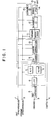
- Bit sync signal 1, frame sync signal 2, sound signal 3 and data 4 are fed to the sender as shown in Figure 1.
- Sound signal 3 is fed to lowpass filter 6 through pre-emphasis circuit 5, and the signal frequency bandwidth is limited by lowpass filter 6.
- the output signal of the lowpass filter is fed to A/D converter 7 and ADM 8 so that the output can be converted into the corresponding digital signal.
- the digital signal and data 4 are fed to encoder 9 so as to convert them into serial data.
- An error correction code is inserted to serial data in error correction code adder 10, and obtained serial data is interleaved by interleaving circuit 11.
- the interleaving circuit output is scrambled by 10th-order polynomial circuit.
- the frame sync signal is also inserted to the scrambled signal in the 1 ⁇ th-order polynomial circuit.
- the RF carrier is frequency-modulated to carry out frequency hopping of the RF carrier in accordance with the frequency hopping pattern obtained by 7th-order polynomial and a sweep pattern.
- Scrambler circuit 13 modulates the RF carrier to perform secondary modulation.
- the RF carrier to which primary modulation is to be accomplished is then fed to phase modulator 14 so that the secondary modulated carrier by the output of scrambler circuit 13 is PSK-modulated by scrambled data fed from scrambler cricuit 12 as the primary modulation.
- the obtained RF carrier signal appears at terminal 15.
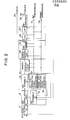
- Received RF signal 16 is fed to acquisition circuit 17 so as to allow the PLL be locked at the designated carrier.
- a certain sync signal is picked up by using both bit sync signal generator 21 and frame sync signal generator 22.
- the hopping pattern is reproduced by using hopping pattern generator 19 so as to keep the PLL locked at the designated carrier.
- a descrambling signal by the 10th-order polynomial is generated by using in descrambler 20 so as to descramble the demodulated serial data.
- the output of descrambler 20 is de-interleaved by using de-interleave circuit 23 and the output of de-interdleave circuit 23 is fed to error correction circuit 24 so as to correct errors, if any.
- the output of error correction circuit 24 is fed to decoder 25 wherein serial data is decoded into the sound PCM signal and data 29.
- the sound PCM signal is fed to D/A converter 26 so that the sound PCM signal is converted into the corresponding audio signal.
- the output of D/A converter 26 is fed through lowpass filter 27 to de-emphasis circuit 28.
- the output of de-emphasis circuit 28 appears at terminal 30.
- One frame consists of 1024 (2 10 ) bits and is composed of eight 128 (2 7 ) bit subframes.
- Signal is scrambled in each frame by 10th-order PN sequence consisting of 1024 bits. Bits 1 through 16 in each frame constitute a specific sync signal which must not be scrambled.
- the frequency-hopped RF carrier is PSK-modulated by the signal scrambled by the 10th-order PN sequence.
- the carrier frequency is hopped in accordance with the frequency hopping pattern consisting of 7th-order 128 bit parallel PN sequences in each subframe.
- Bits 1 through 16 of the first subframe in each frame are used to help the PLL be locked in the receiver at the designated carrier.
- the carrier frequncy is swept in such a digital manner as shown in Figure 4, and bits 1 through 16 of the first subframe cannot be used as part of the 7th-order frequency hopping pattern of the PN sequence.
- Signals are scrambled by the frequency hopping patterns whose frequencies are shifted in accordance with the duplex PN sequences consisting of 1024 (2 10 ) bits in each frame and of 128 (2 7 ) bits in each subframe.
- Eight repetitive frequency hopping patterns, each having a period of a subframe, can appear in a frame.
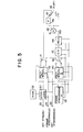
- Figure 5 shows a block diagram of the modulator.
- the PN sequence of a 7th order polynomial is generated by using PN generator circuit 40, synchronizing with the bit and frame sync signals.
- Subframes having a period of 128 bits are repeated eight times in the PN sequence within a frame consisting of 1024 bits.
- Bits 1 through 16 of each frame in the frequency hopping pattern constitute a sweep pattern signal for acquisition of the carrier in the receiver, and the sweep pattern signal is supplied from frame sync controller 38.
- Either the frequency hopping pattern signal or the sweep pattern signal is selected by switch 42, and the selected signal is fed to D/A converter 43.
- the sweep pattern signal is fed from frame sync controller 38 to D/A converter 43 if switch 42 is set at position "b". Bits 1 through 16 of each frame are then designated for use.
- the frequency hopping pattern signal for the PN sequence of the 7th-order polynomial is fed to D/A converter 43 if switch 42 is set at position "a". Bits 17 through 1024 of each frame are then designated for use.
- switch 42 When frequency hopping for a frame is completed, switch 42 is set at position "b". Thereafter, the same operations as above are repeated.
- the frequency hopping pattern signal passing through D/A converter 43 is fed to hold circuit 44 so as to shape the signal waveform, and then the output of hold circuit 44 is fed to VCO 45.
- the frequency hopping pattern signal is fed from hold circuit 44 to VCO 45 and is used to perform frequency modulation in VCO 45.
- the frequency-hopped carrier or spread spectrum carrier is generated by using VCO 45.
- PSK modulation is carried out to the carrier by using phase shifter 46. That is, the output of VCO 45 branches into two routes. One leads to positon "b" of switch 47, and the other to position "a” of switch 47 passing through phase shifter 46 which shifts the carrier phase by 180 degrees.
- the interleaved signal is scrambled by the 10th-order polynomial of the PN sequence tracked into the frame bits.
- Figure 6 shows the demodulator used in the spread spectrum communication system in accordance with the present invention.
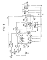
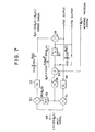
- Figure 7 shows the Costas loop PLL in the receiver used in the spread spectrum communication system.
- Input signal I ⁇ A cos ⁇ a(t) is applied to input terminal 49. Signs+ and - correspond to 1 and 0 of the binary data modulation, respectively.
- Input signal branches into two routes. One leads to multiplier 50 and the other to multiplier 51. Signal cos ⁇ b(t) is fed from VCO 53 to multiplier 50 through x/2-phase shifter 52. Input signal ⁇ A cos ⁇ a(t) is then multiplied by signal sin ⁇ b(t). Signal cos ⁇ b(t) is directly fed from VCO 53 to multiplier 51. Input signal ⁇ A cos ⁇ a(t) is then multiplied by signal cos ⁇ b(t).
- multipliers 50 and 51 are fed to lowpass filters 55 and 56 so that a pair of phase error components with phases orthogonal to each other are produced.
- the orthogonal components are multiplied by multiplier 59 and resultant phase error signal Ep becomes
- Phase error signal Ep is fed through filter 57 to adder 54 so as to add hopping pattern signal ⁇ d(t) to phase error signal Ep.
- the result of addition in adder 54 is fed to VCO 53 so as to control instantaneous angular frequency d ⁇ d(t)/dt of the signal generated by VCO 53.
- the left-hand side of Eq. (2) indicates the instantaneous angular frequency of the phase error
- the first term in the right-hand side indicates the instantaneous angular frequency of the input signal
- the second term in the right-hand side indicates the frequency hopping pattern
- the third term in the right-hand side indicates the free run frequency of the VCO
- the fourth term in the right-hand side indicates the phase error signal fed from the loop filter.
- frequency hopping pattern signal ,d(t) applied to adder 54 should be tracked into the frequency hopping pattern of the input signal.
- bit and frame sync signals should have been picked up.
- bit sync signal is being picked up by using PLL 66 shown in Figure 6.
- the frequency hopping pattern may be demodulated to pick up these sync signals by the normal Costas loop with higher loop gain and with the loop filter having higher cutoff frequency.
- the loop filter has higher cutoff frequency and thus the PLL goes into the stationary state within a short time.
- Equation (4) in this state is given by
- Phase error ⁇ c(t) then becomes constant value ⁇ k, and sin ⁇ k is given by
- the phase error signal is proportional to the difference between angular frequency ⁇ a of the input signal and free run frequency ⁇ f of the VCO 53 in the stationary state while the PLL is being tracked into the input signal.
- Acquisition is an operation to pick up the frame sync signal from the output of the FM demodulator in this state.
- the phase error signal becomes zero only when angular frequency ⁇ a of the input signal coincides with free run frequency ⁇ f of the VCO 53.
- loop filter 57 has an extremely low cutoff frequency or inpulse response h(t) exists for a long period of time.
- the delay time within a loop is mainly determined by multiplier 59.
- Long delay time causes the PLL operation to be unstable especially when the loop gain is high.
- Wide lock range is favorable to acquisition operation.
- the lock range should be set narrow if excellent anti-interference performance is required.
- the lock range needs not be wide in the steady tracking state where the frequency of the PLL is tracked into the input signal in the previously described manner.
- the receiver consists of a PLL constructed with elements identified by 49 through 61, forming a costas loop, correlator 62 for use to pick up the sweep pattern, a frequency hopping pattern generator constructed with elements identified by 63 through 65, and a digital signal processor constructed with elements identified by 66 through 76.
- switch 60 of the PLL in the costas loop is set at position "a" and that switch 61 is open. Then, the system is held in the acquisition during initial phase.
- Lowpass filters 55 and 56 for use to cutoff the RF components have higher cutoff frequencies, respectively. These filters have short delay times at the baseband frequencies.
- the frequency response of multiplier 59 is almost the same as that of a video amplifier and multiplier 59 has a short delay time.
- the gain of multiplier 59 is set so that the lock range of the PLL in the Costas loop covers the bandwidth of spread spectrum due to secondary modulation of the carrier signal. From Eq. (6), the lock range is given by
- the lock range can be spreaded by increasing the input signal amplitude or by increasing the loop gain.
- a Costas loop with longer delay time makes the system unstable.
- the loop .gain cannot be increased and thus the lock range cannot be spreaded in such a case.
- the circuit parameter is therefore selected so that the delay time of the circuit within a loop is short in the acquisition state, and the lock range is wide enough to allow the PLL to be tracked into the input signal.
- the PLL is locked into the carrier to which secondary modulation is accomplished.
- the FM-demodulated signal which is the frequency hopping pattern or secondary-modulated signal can be obtained from multiplier 59.
- the output of multiplier 59 is fed to correlator 62 which is used to pick up the frequency sweep signal or frame sync pattern.
- the PSK-demodulated signal or primary-modulated signal is obtained from multiplier 51, forming the I axis of the Costas loop, and the output of multiplier 51 is fed through lowpass filter 56 to PLL 66 designated as VCXO for use to pick up the bit sync signal.
- PLL 66 has a short lock-in time starting with the beginning of a lock-in operation until the system enters the acquisition operation. The lock-in time measures five to six bits or less.
- Correlator 62 for use to pick up the frequency sweep signal is operated by the bit sync signal obtained in accordance with the above operations.
- Correlator 62 eliminating noises and unwanted interference signals, picks up a hopping pattern whose differentials are the same in sign for a certain bit length so as to detect the frequency sweep pattern.
- the primary-modulated signal is demodulated in accordance with the PSK-demodulted signal while the bit sync signal has been extracted from the PSK-demodulated signal.
- Integrate and dump filter 67 which is operated in accordance with the bit sync signal, eliminates noises and unwanted interference signals.
- the output of integrate and dump filter 67 is fed to both controller 69 and descramble circuit 70.
- controller 69 determines the location of the frame and detects a zero in bit 16 of the first frame or the last bit of the PSK-demodulated frame sync signal.
- controller 69 causes descramble circuit 70, frequency hopping signal reproduction circuit 68, and de-interleave circuit 71 to start operating.
- the PN sequence generation circuits operated in accordance with the 1 ⁇ th-order and 7th-order polynomials in descramble circuit 70 and frequency hopping reproduction circuit 68 are the same as those in the sender, respectively.
- the loop constant in which the PLL can be tracked into the input signal is unchanged during first frame demodulation, descramble operations, and during frequency hopping pattern signal generation.
- controller 69 changes the positions of switches 60 and 61 so as to change the loop constant in bit 8 or bit 9 when the frequency sweep pattern in the frame sync signal approaches the free run frequency of the VCO 53 in the Costas loop. That is, switch 60 is set at position "b" and switch 61 is closed.
- the loop circuit consists of attenuator 58, loop filter 57 and adder 54.
- the cutoff frequency of loop filter 57 is set low so that the loop circuit is stable against interferences.
- Adder 54 is made by using an operational amplifier having longer delay time.
- attenuator 58 is used to decrease the loop gain because higher loop gain would make the loop circuit unstable.
- the offset signal for the frequency hopping pattern generated by using D/A converter 64 before the positions of switches 60 and 61 are changed is fed to adder 54.
- the frequency sweep pattern approaches the free run frequency of VCO 53 in the Costas loop at bit 8 or bit 9.
- the phase error signal issued from multiplier 59 approaches zero and no significant transient response can be induced by loop filter 57 even if the loop constant is changed.
- the Costas loop follows the fictitious carrier at which no PSK-modulated phase information is contained as Eq. (2), (3) or (4) shows.
- the cutoff frequency of loop filter 57 can arbitrarily be decreased so as to pick up the carrier containing no information, which enables the Costas loop to possess excellent anti-interference performance.
- the PSK-demodulated signal issued onto the I-axis of the Costas loop is correlated by using integrate and dump filter 67 so as to stably extract the modulation signal.
- phase error signal is always approximately zero independent of the loop constant and the loop constant can easily be changed.
- a loop filter having a narrow bandwidth can be used for the PLL in the same manner as in the SS system of direct sequence spread spectrum communication.
- the circuit can be simplified and superior performance to protect the communication against interference can be realized.
Abstract
Description
- The present invention relates to the spread spectrum communication system, and especially to the the spread spectrum communication system wherein the offset voltage pattern of frequency hopping is applied to the VCO of the PLL in the receiver thereof.
- A plurality of synthesizer outputs are combined together with the carrier signal in the conventional spread spectrum communication system realized by frequency hopping, and thus a plurality of discontinuous points have occurred in the carrier phase domain. No receiver employing the coherent detection system is suitable for the spread spectrum communication system realized by frequency hopping and, especially in case that the receiver can operate for high speed data transmission, this type of receiver cannot be used for the spread spectrum communication system realized by frequency hopping.
- A receiver employing an incoherent detection system has a circuit configuration complicated. Spans between adjacent carriers in the frequency domain are not arbitrary and anti-interference performance obtained by incoherent detection is normally inferior to that obtained by coherent detection.
- The objective of the present invention is to present means to make it possible for the spread spectrum communication system realized by frequency hopping to peform coherent detection with a simple detection circuit so that performance of the receiver realized by employing the coherent detection system is superior than that realized by employing the incoherent detection system.
- The spread spectrum communication system realized by frequency hopping in accordance with the present invention employs a coherent detection system, wherein the offset voltage pattern pre-determined by a certain polynomial is applied to the VCO of the PLL in the receiver thereof so that the PLL can be operated with a narrow bandwidth because of the narrow bandwidth of the loop filter as well as a decreased loop gain while avoiding tracking break caused by narrow lock range due to the narrow bandwidth of the loop filter as well as the decreased loop gain.
-
- Figure 1 is a block diagram of the sender in the spread spectrum communication system in accordance with the present invention.
- Figure 2 is a block diagram of the receiver in the spread spectrum communication system in accordance with the present invention.
- Figure 3 shows a signal frame format used in the spread spectrum communication system in accordance with the present invention.
- Figure 4 shows a signal frame pattern in detail.
- Figure 5 is a block diagram of the modulator used in the spread spectrum communication system in accordance with the present invention.
- Figure 6 shows the demodulator used in the spread spectrum communication system in accordance with the present invention.
- Figure 7 shows the Costas loop PLL in the receiver used in the spread spectrum communication system.
- The present invention will be described hereafter referring to the attached drawings.
-
Bit sync signal 1,frame sync signal 2,sound signal 3 anddata 4 are fed to the sender as shown in Figure 1. -
Sound signal 3 is fed tolowpass filter 6 through pre-emphasiscircuit 5, and the signal frequency bandwidth is limited bylowpass filter 6. The output signal of the lowpass filter is fed to A/D converter 7 andADM 8 so that the output can be converted into the corresponding digital signal. - The digital signal and
data 4 are fed toencoder 9 so as to convert them into serial data. - An error correction code is inserted to serial data in error
correction code adder 10, and obtained serial data is interleaved by interleaving circuit 11. The interleaving circuit output is scrambled by 10th-order polynomial circuit. The frame sync signal is also inserted to the scrambled signal in the 1θth-order polynomial circuit. - The RF carrier is frequency-modulated to carry out frequency hopping of the RF carrier in accordance with the frequency hopping pattern obtained by 7th-order polynomial and a sweep pattern.
-
Scrambler circuit 13 modulates the RF carrier to perform secondary modulation. The RF carrier to which primary modulation is to be accomplished is then fed tophase modulator 14 so that the secondary modulated carrier by the output ofscrambler circuit 13 is PSK-modulated by scrambled data fed from scrambler cricuit 12 as the primary modulation. The obtained RF carrier signal appears atterminal 15. - The receiver will be described hereafter referring to Figure 2. Received
RF signal 16 is fed toacquisition circuit 17 so as to allow the PLL be locked at the designated carrier. A certain sync signal is picked up by using both bitsync signal generator 21 and framesync signal generator 22. The hopping pattern is reproduced by usinghopping pattern generator 19 so as to keep the PLL locked at the designated carrier. At the same time, a descrambling signal by the 10th-order polynomial is generated by using indescrambler 20 so as to descramble the demodulated serial data. - Thereafter, the output of
descrambler 20 is de-interleaved by using de-interleavecircuit 23 and the output of de-interdleavecircuit 23 is fed toerror correction circuit 24 so as to correct errors, if any. The output oferror correction circuit 24 is fed todecoder 25 wherein serial data is decoded into the sound PCM signal anddata 29. The sound PCM signal is fed to D/A converter 26 so that the sound PCM signal is converted into the corresponding audio signal. The output of D/A converter 26 is fed throughlowpass filter 27 to de-emphasiscircuit 28. The output of de-emphasiscircuit 28 appears atterminal 30. - The signal frame format in the SS system realized in accordance with the present invention will be described referring to Figure 3.
- One frame consists of 1024 (210) bits and is composed of eight 128 (27 ) bit subframes.
- Signal is scrambled in each frame by 10th-order PN sequence consisting of 1024 bits.
Bits 1 through 16 in each frame constitute a specific sync signal which must not be scrambled. - The frequency-hopped RF carrier is PSK-modulated by the signal scrambled by the 10th-order PN sequence.
- The carrier frequency is hopped in accordance with the frequency hopping pattern consisting of 7th-
order 128 bit parallel PN sequences in each subframe. -
Bits 1 through 16 of the first subframe in each frame are used to help the PLL be locked in the receiver at the designated carrier. The carrier frequncy is swept in such a digital manner as shown in Figure 4, andbits 1 through 16 of the first subframe cannot be used as part of the 7th-order frequency hopping pattern of the PN sequence. - Signals are scrambled by the frequency hopping patterns whose frequencies are shifted in accordance with the duplex PN sequences consisting of 1024 (210) bits in each frame and of 128 (27) bits in each subframe. Eight repetitive frequency hopping patterns, each having a period of a subframe, can appear in a frame.
- The modulator and demodulator which are used in the spread spectrum communication system in accordance with the present invention will be described hereafter.
- Figure 5 shows a block diagram of the modulator.
- First, carrier frequency hopping will be described.
- The PN sequence of a 7th order polynomial is generated by using
PN generator circuit 40, synchronizing with the bit and frame sync signals. - Subframes having a period of 128 bits are repeated eight times in the PN sequence within a frame consisting of 1024 bits.
Bits 1 through 16 of each frame in the frequency hopping pattern constitute a sweep pattern signal for acquisition of the carrier in the receiver, and the sweep pattern signal is supplied fromframe sync controller 38. - Either the frequency hopping pattern signal or the sweep pattern signal is selected by
switch 42, and the selected signal is fed to D/A converter 43. - The sweep pattern signal is fed from
frame sync controller 38 to D/A converter 43 ifswitch 42 is set at position "b".Bits 1 through 16 of each frame are then designated for use. - The frequency hopping pattern signal for the PN sequence of the 7th-order polynomial is fed to D/
A converter 43 ifswitch 42 is set at position "a".Bits 17 through 1024 of each frame are then designated for use. - When frequency hopping for a frame is completed,
switch 42 is set at position "b". Thereafter, the same operations as above are repeated. - The frequency hopping pattern signal passing through D/
A converter 43 is fed to holdcircuit 44 so as to shape the signal waveform, and then the output ofhold circuit 44 is fed toVCO 45. - The frequency hopping pattern signal is fed from
hold circuit 44 toVCO 45 and is used to perform frequency modulation inVCO 45. The frequency-hopped carrier or spread spectrum carrier is generated by usingVCO 45. - PSK modulation is carried out to the carrier by using
phase shifter 46. That is, the output ofVCO 45 branches into two routes. One leads to positon "b" ofswitch 47, and the other to position "a" ofswitch 47 passing throughphase shifter 46 which shifts the carrier phase by 180 degrees. - The interleaved signal is scrambled by the 10th-order polynomial of the PN sequence tracked into the frame bits.
- Figure 6 shows the demodulator used in the spread spectrum communication system in accordance with the present invention.
- Figure 7 shows the Costas loop PLL in the receiver used in the spread spectrum communication system.
- Input signal I = ± A cos φa(t) is applied to input terminal 49. Signs+ and - correspond to 1 and 0 of the binary data modulation, respectively.
- Input signal branches into two routes. One leads to
multiplier 50 and the other tomultiplier 51. Signal cos φb(t) is fed fromVCO 53 tomultiplier 50 through x/2-phase shifter 52. Input signal ±A cos φa(t) is then multiplied by signal sin φb(t). Signal cos φb(t) is directly fed fromVCO 53 tomultiplier 51. Input signal ± A cos φa(t) is then multiplied by signal cos φb(t). - The outputs of
multipliers lowpass filters multiplier 59 and resultant phase error signal Ep becomes -

- Phase error signal Ep is fed through
filter 57 to adder 54 so as to add hopping pattern signal φd(t) to phase error signal Ep. The result of addition inadder 54 is fed toVCO 53 so as to control instantaneous angular frequency d φd(t)/dt of the signal generated byVCO 53. - If
adder 54 were not installed and no hopping pattern signal φd(t) were added to phase error signal Ep, the normal costas loop would be established. - The above operation is expressed by Eq. (2).

- The left-hand side of Eq. (2) indicates the instantaneous angular frequency of the phase error, the first term in the right-hand side indicates the instantaneous angular frequency of the input signal, the second term in the right-hand side indicates the frequency hopping pattern, the third term in the right-hand side indicates the free run frequency of the VCO, and the fourth term in the right-hand side indicates the phase error signal fed from the loop filter.
- If instantaneous angular frequency d φa(t)/dt of the input signal is equal to the sum of angular frequency ωf of free run frequency of the VCO and frequency hopping pattern signal φd(t), equation (2) becomes
-

- The right-hand side term of expression (3) approaches asymptotically to zero when "t" becomes infinity.
- d φc(t)/dt is held zero in this state, and thus the loop is kept stationary. The system can thus be kept stationary even if the carrier frequency is hopped. Thus, the cutoff frequency of the loop filter can arbitrarily be set low and the carrier can be reproduced satisfactorily even if interference is great.
- For successful operation, frequency hopping pattern signal ,d(t) applied to adder 54 should be tracked into the frequency hopping pattern of the input signal. For satisfactory tracking, the bit and frame sync signals should have been picked up.
- First, the bit sync signal is being picked up by using
PLL 66 shown in Figure 6. - The frequency hopping pattern may be demodulated to pick up these sync signals by the normal Costas loop with higher loop gain and with the loop filter having higher cutoff frequency.
- Assume that
switch 60 is set at position "a", and thatswitch 61 is open. Then, the frame sync signal is picked up bycorrelator 62 which is used to pick up the sweep pattern signal for frame synchronization. - The loop filter has higher cutoff frequency and thus the PLL goes into the stationary state within a short time.
- The above operation is expressed as
-

- The instantaneous angular frequency of the
VCO 53 thus agrees with angular frequency ωa of the input signal. Equation (4) in this state is given by
- Phase error φc(t) then becomes constant value φk, and sin φk is given by

- The phase error signal is proportional to the difference between angular frequency Φa of the input signal and free run frequency Φf of the
VCO 53 in the stationary state while the PLL is being tracked into the input signal. - Acquisition is an operation to pick up the frame sync signal from the output of the FM demodulator in this state.
- As described in equation (6), the phase error signal becomes zero only when angular frequency Φa of the input signal coincides with free run frequency ωf of the
VCO 53. The phase error signal is other than zero in the other state, and φk = ± π/2 at the edge of the lock range. - When the Costas loop is changed from the acquisition state to the steady tracking state by changing positions of
switches loop filter 57 has an extremely low cutoff frequency or inpulse response h(t) exists for a long period of time. - When the same operation is performed if φk ≠ 0, the system starts operating with the steady state and the system stays stable.
- From the circuit realization point of view, the delay time within a loop is mainly determined by
multiplier 59. Long delay time causes the PLL operation to be unstable especially when the loop gain is high. The higher the loop gain becomes, the wider the lock range becomes. Wide lock range is favorable to acquisition operation. - When the positions of
switches - From the circuit realization point of view, and from the SS system realization point of view, it is reasonable for the Costas loop to have a loop constant which can be changed in accordance with the state of whether the costas loop is used for acquisition or for steady tracking state. The receiver consists of a PLL constructed with elements identified by 49 through 61, forming a costas loop,
correlator 62 for use to pick up the sweep pattern, a frequency hopping pattern generator constructed with elements identified by 63 through 65, and a digital signal processor constructed with elements identified by 66 through 76. - Assume that
switch 60 of the PLL in the costas loop is set at position "a" and thatswitch 61 is open. Then, the system is held in the acquisition during initial phase. - Lowpass filters 55 and 56 for use to cutoff the RF components have higher cutoff frequencies, respectively. These filters have short delay times at the baseband frequencies. The frequency response of
multiplier 59 is almost the same as that of a video amplifier andmultiplier 59 has a short delay time. The gain ofmultiplier 59 is set so that the lock range of the PLL in the Costas loop covers the bandwidth of spread spectrum due to secondary modulation of the carrier signal. From Eq. (6), the lock range is given by -


- The lock range can be spreaded by increasing the input signal amplitude or by increasing the loop gain.
- A Costas loop with longer delay time makes the system unstable. The loop .gain cannot be increased and thus the lock range cannot be spreaded in such a case. The circuit parameter is therefore selected so that the delay time of the circuit within a loop is short in the acquisition state, and the lock range is wide enough to allow the PLL to be tracked into the input signal. When the input signal is fed to the PLL in the Costas loop in the above state, the PLL is locked into the carrier to which secondary modulation is accomplished. Then, the FM-demodulated signal which is the frequency hopping pattern or secondary-modulated signal can be obtained from
multiplier 59. The output ofmultiplier 59 is fed to correlator 62 which is used to pick up the frequency sweep signal or frame sync pattern. At that time, the PSK-demodulated signal or primary-modulated signal is obtained frommultiplier 51, forming the I axis of the Costas loop, and the output ofmultiplier 51 is fed throughlowpass filter 56 toPLL 66 designated as VCXO for use to pick up the bit sync signal.PLL 66 has a short lock-in time starting with the beginning of a lock-in operation until the system enters the acquisition operation. The lock-in time measures five to six bits or less. Thus, the bit sync signal can be obtained before the frame sync signal is picked up.Correlator 62 for use to pick up the frequency sweep signal is operated by the bit sync signal obtained in accordance with the above operations. -
Correlator 62, eliminating noises and unwanted interference signals, picks up a hopping pattern whose differentials are the same in sign for a certain bit length so as to detect the frequency sweep pattern. - In addition, the primary-modulated signal is demodulated in accordance with the PSK-demodulted signal while the bit sync signal has been extracted from the PSK-demodulated signal.
- Integrate and dump
filter 67, which is operated in accordance with the bit sync signal, eliminates noises and unwanted interference signals.. The output of integrate and dumpfilter 67 is fed to bothcontroller 69 and descramblecircuit 70. Upon receipt of the frequency sweep signal representing that the frame sync signal has been picked up,controller 69 determines the location of the frame and detects a zero inbit 16 of the first frame or the last bit of the PSK-demodulated frame sync signal. Whenbit 17 of the first frame is recognized,controller 69 causes descramblecircuit 70, frequency hoppingsignal reproduction circuit 68, and de-interleave circuit 71 to start operating. - The PN sequence generation circuits operated in accordance with the 1θth-order and 7th-order polynomials in
descramble circuit 70 and frequency hoppingreproduction circuit 68 are the same as those in the sender, respectively. - The loop constant in which the PLL can be tracked into the input signal is unchanged during first frame demodulation, descramble operations, and during frequency hopping pattern signal generation.
- When demodulation of the carrier signals in the second frame starts after demodulation of the carrier signals in the first frame is completed,
controller 69 changes the positions ofswitches bit 8 orbit 9 when the frequency sweep pattern in the frame sync signal approaches the free run frequency of theVCO 53 in the Costas loop. That is,switch 60 is set at position "b" and switch 61 is closed. - The loop circuit consists of
attenuator 58,loop filter 57 andadder 54. - The cutoff frequency of
loop filter 57 is set low so that the loop circuit is stable against interferences.Adder 54 is made by using an operational amplifier having longer delay time. Thus,attenuator 58 is used to decrease the loop gain because higher loop gain would make the loop circuit unstable. - The offset signal for the frequency hopping pattern generated by using D/
A converter 64 before the positions ofswitches - Assume that an error signal in a certain level is fed to
multiplier 54 while the loop constant is being changed by changing the positions ofswitches loop filter 57 is set low and that the loop gain is set low. Because of low cutoff frequency and low loop gain, the PLL would go out of the lock range and the PLL should have longer lock-in time. - The frequency sweep pattern approaches the free run frequency of
VCO 53 in the Costas loop atbit 8 orbit 9. The phase error signal issued frommultiplier 59 approaches zero and no significant transient response can be induced byloop filter 57 even if the loop constant is changed. - As described by Eq. (3), if input signal sin c(t) fed to
loop filter 57 is zero for -∞<t<t1, φc(t) = 0 is maintained for t>t1 . Then, the costas loop remains in the steady state independent of carrier frequency hopping due to secondary modulation. - The Costas loop follows the fictitious carrier at which no PSK-modulated phase information is contained as Eq. (2), (3) or (4) shows. Thus, the cutoff frequency of
loop filter 57 can arbitrarily be decreased so as to pick up the carrier containing no information, which enables the Costas loop to possess excellent anti-interference performance. When the carrier is stably picked up, the PSK-demodulated signal issued onto the I-axis of the Costas loop is correlated by using integrate and dumpfilter 67 so as to stably extract the modulation signal. - In the SS system wherein the carrier frequency is unchanged to perform direct sequence spread spectrum communication, the phase error signal is always approximately zero independent of the loop constant and the loop constant can easily be changed.
- In the frequency hopping system wherein frequencies are more effectively used than in the direct sequence system, a loop filter having a narrow bandwidth can be used for the PLL in the same manner as in the SS system of direct sequence spread spectrum communication. Thus, the circuit can be simplified and superior performance to protect the communication against interference can be realized.
Claims (3)
- (1) Spread spectrum communication system, wherein carriers are modulated and demodulated by using the frequency hopping coherent detection system.
- (2) Spread spectrum communication system as claimed in Claim (1), wherein such an offset voltage pattern as pre-determined by the frequency hopping signal reproduction circuit is applied to a PLL in the receiver thereof, so that the PLL can be constructed with a loop filter of narrow bandwidth as well as a decreased loop gain while avoiding tracking break caused by narrow lock range due to said narrow bandwidth as well as said decreased loop gain.
- (3) Spread spectrum communication system as claimed in Claim (1), wherein a Costas loop establishes a normal bandwidth loop or a narrow bandwidth loop wherein the frequency hopping offset signal can be added to the phase error signal, which can selectively be used to stably operate the system, and a controller is used to start generation of both the frequency hopping pattern and PN pattern for use in de-scramble operations in the first frame while the frame sync signal and the bit sync signal for the acquisition are extracted from the PSK and FM demodulated signals by locking the Costas loop into the input signal, and then to change the loop constant from said normal bandwidth loop to said narrow bandwidth loop in the second frame while the frame sync signal and the bit sync signal are extracted from the PSK and FM demodulated signals for the steady tracking state by locking the Costas loop into the input signal.
Applications Claiming Priority (2)
| Application Number | Priority Date | Filing Date | Title |
|---|---|---|---|
| JP280988/84 | 1984-12-29 | ||
| JP59280988A JPH0693670B2 (en) | 1984-12-29 | 1984-12-29 | Spread spectrum communication system |
Publications (3)
| Publication Number | Publication Date |
|---|---|
| EP0186884A2 true EP0186884A2 (en) | 1986-07-09 |
| EP0186884A3 EP0186884A3 (en) | 1988-09-21 |
| EP0186884B1 EP0186884B1 (en) | 1992-09-02 |
Family
ID=17632688
Family Applications (1)
| Application Number | Title | Priority Date | Filing Date |
|---|---|---|---|
| EP85116432A Expired - Lifetime EP0186884B1 (en) | 1984-12-29 | 1985-12-21 | Spread spectrum communication system |
Country Status (4)
| Country | Link |
|---|---|
| US (1) | US4760586A (en) |
| EP (1) | EP0186884B1 (en) |
| JP (1) | JPH0693670B2 (en) |
| DE (1) | DE3586586D1 (en) |
Cited By (2)
| Publication number | Priority date | Publication date | Assignee | Title |
|---|---|---|---|---|
| EP0208915A1 (en) * | 1985-07-19 | 1987-01-21 | ANT Nachrichtentechnik GmbH | Method for demodulating a frequency and phaseshift keyed signal |
| GB2379105A (en) * | 2001-08-24 | 2003-02-26 | Roke Manor Research | Improvements in or relating to fast frequency-hopping modulators and demodulators |
Families Citing this family (52)
| Publication number | Priority date | Publication date | Assignee | Title |
|---|---|---|---|---|
| JPH07123232B2 (en) * | 1986-08-06 | 1995-12-25 | 京セラ株式会社 | Synchronous tracking device for spread spectrum communication |
| JPS6393233A (en) * | 1986-10-08 | 1988-04-23 | Oki Electric Ind Co Ltd | Spread spectrum communication system |
| US4888788A (en) * | 1986-11-20 | 1989-12-19 | Matsushita Electric Industrial Co., Ltd. | Transmitting and receiving systems |
| JPH01151843A (en) * | 1987-12-09 | 1989-06-14 | Nec Corp | Spread spectrum demodulator |
| US4964138A (en) * | 1988-11-15 | 1990-10-16 | Agilis Corporation | Differential correlator for spread spectrum communication system |
| US4968970A (en) * | 1989-04-26 | 1990-11-06 | Schlumberger Industries, Inc. | Method of and system for power line carrier communications |
| US5276703A (en) * | 1992-01-13 | 1994-01-04 | Windata, Inc. | Wireless local area network communications system |
| SG52170A1 (en) * | 1994-02-17 | 1998-09-28 | Micrilor Inc | A high-data-rate wireless local-area network |
| US5970400A (en) * | 1996-04-30 | 1999-10-19 | Magellan Corporation | Adjusting the timing and synchronization of a radio's oscillator with a signal from an SATPS satellite |
| KR100217413B1 (en) * | 1996-08-24 | 1999-09-01 | 윤종용 | Wireless communltication system of using time division duplexing/frequecy hopping mehtod |
| US6865216B1 (en) * | 1998-08-20 | 2005-03-08 | Skyworks Solutions Inc. | Frequency hopping spread spectrum modulation and direct sequence spread spectrum modulation cordless telephone |
| US6498784B1 (en) * | 1998-10-20 | 2002-12-24 | Interdigital Technology Corporation | Cancellation of pilot and traffic signals |
| US6714085B1 (en) | 2002-10-24 | 2004-03-30 | General Dynamics Decision Systems, Inc | Prepositioned frequency synthesizer and method therefor |
| US20050059406A1 (en) * | 2003-09-17 | 2005-03-17 | Trapeze Networks, Inc. | Wireless LAN measurement feedback |
| US20050059405A1 (en) * | 2003-09-17 | 2005-03-17 | Trapeze Networks, Inc. | Simulation driven wireless LAN planning |
| US7221927B2 (en) * | 2004-02-13 | 2007-05-22 | Trapeze Networks, Inc. | Station mobility between access points |
| WO2006099540A2 (en) | 2005-03-15 | 2006-09-21 | Trapeze Networks, Inc. | System and method for distributing keys in a wireless network |
| US7551619B2 (en) | 2005-10-13 | 2009-06-23 | Trapeze Networks, Inc. | Identity-based networking |
| US7573859B2 (en) | 2005-10-13 | 2009-08-11 | Trapeze Networks, Inc. | System and method for remote monitoring in a wireless network |
| US8638762B2 (en) | 2005-10-13 | 2014-01-28 | Trapeze Networks, Inc. | System and method for network integrity |
| US7724703B2 (en) | 2005-10-13 | 2010-05-25 | Belden, Inc. | System and method for wireless network monitoring |
| WO2007044986A2 (en) * | 2005-10-13 | 2007-04-19 | Trapeze Networks, Inc. | System and method for remote monitoring in a wireless network |
| US8250587B2 (en) | 2005-10-27 | 2012-08-21 | Trapeze Networks, Inc. | Non-persistent and persistent information setting method and system for inter-process communication |
| US7558266B2 (en) * | 2006-05-03 | 2009-07-07 | Trapeze Networks, Inc. | System and method for restricting network access using forwarding databases |
| US20070260720A1 (en) * | 2006-05-03 | 2007-11-08 | Morain Gary E | Mobility domain |
| US8966018B2 (en) | 2006-05-19 | 2015-02-24 | Trapeze Networks, Inc. | Automated network device configuration and network deployment |
| US20070268516A1 (en) * | 2006-05-19 | 2007-11-22 | Jamsheed Bugwadia | Automated policy-based network device configuration and network deployment |
| US20070268515A1 (en) * | 2006-05-19 | 2007-11-22 | Yun Freund | System and method for automatic configuration of remote network switch and connected access point devices |
| US20070268506A1 (en) * | 2006-05-19 | 2007-11-22 | Paul Zeldin | Autonomous auto-configuring wireless network device |
| US20070268514A1 (en) * | 2006-05-19 | 2007-11-22 | Paul Zeldin | Method and business model for automated configuration and deployment of a wireless network in a facility without network administrator intervention |
| US7577453B2 (en) * | 2006-06-01 | 2009-08-18 | Trapeze Networks, Inc. | Wireless load balancing across bands |
| US7912982B2 (en) | 2006-06-09 | 2011-03-22 | Trapeze Networks, Inc. | Wireless routing selection system and method |
| US9258702B2 (en) | 2006-06-09 | 2016-02-09 | Trapeze Networks, Inc. | AP-local dynamic switching |
| US8818322B2 (en) | 2006-06-09 | 2014-08-26 | Trapeze Networks, Inc. | Untethered access point mesh system and method |
| US9191799B2 (en) | 2006-06-09 | 2015-11-17 | Juniper Networks, Inc. | Sharing data between wireless switches system and method |
| US7844298B2 (en) | 2006-06-12 | 2010-11-30 | Belden Inc. | Tuned directional antennas |
| US7724704B2 (en) | 2006-07-17 | 2010-05-25 | Beiden Inc. | Wireless VLAN system and method |
| US8340110B2 (en) | 2006-09-15 | 2012-12-25 | Trapeze Networks, Inc. | Quality of service provisioning for wireless networks |
| US8072952B2 (en) | 2006-10-16 | 2011-12-06 | Juniper Networks, Inc. | Load balancing |
| US20080107077A1 (en) * | 2006-11-03 | 2008-05-08 | James Murphy | Subnet mobility supporting wireless handoff |
| US7865713B2 (en) | 2006-12-28 | 2011-01-04 | Trapeze Networks, Inc. | Application-aware wireless network system and method |
| US7873061B2 (en) | 2006-12-28 | 2011-01-18 | Trapeze Networks, Inc. | System and method for aggregation and queuing in a wireless network |
| US8902904B2 (en) | 2007-09-07 | 2014-12-02 | Trapeze Networks, Inc. | Network assignment based on priority |
| US8509128B2 (en) | 2007-09-18 | 2013-08-13 | Trapeze Networks, Inc. | High level instruction convergence function |
| US8238942B2 (en) | 2007-11-21 | 2012-08-07 | Trapeze Networks, Inc. | Wireless station location detection |
| US8150357B2 (en) | 2008-03-28 | 2012-04-03 | Trapeze Networks, Inc. | Smoothing filter for irregular update intervals |
| US8474023B2 (en) | 2008-05-30 | 2013-06-25 | Juniper Networks, Inc. | Proactive credential caching |
| US8978105B2 (en) | 2008-07-25 | 2015-03-10 | Trapeze Networks, Inc. | Affirming network relationships and resource access via related networks |
| US8238298B2 (en) | 2008-08-29 | 2012-08-07 | Trapeze Networks, Inc. | Picking an optimal channel for an access point in a wireless network |
| US8542836B2 (en) | 2010-12-01 | 2013-09-24 | Juniper Networks, Inc. | System, apparatus and methods for highly scalable continuous roaming within a wireless network |
| US20140036332A1 (en) * | 2012-08-01 | 2014-02-06 | Digital Signal Corporation | System and Method for Positioning a Mirror in a Lidar System Using Open Loop and Closed Loop Control |
| JP5663633B2 (en) * | 2013-07-12 | 2015-02-04 | 株式会社日立製作所 | GPS signal transmitter and signal transmission method thereof |
Citations (2)
| Publication number | Priority date | Publication date | Assignee | Title |
|---|---|---|---|---|
| US3983501A (en) * | 1975-09-29 | 1976-09-28 | The United States Of America As Represented By The Secretary Of The Navy | Hybrid tracking loop for detecting phase shift keyed signals |
| DE2631460B1 (en) * | 1976-07-13 | 1977-06-08 | Siemens Ag | Circuit arrangement for generating a control signal in a receiving channel prone to interference |
Family Cites Families (8)
| Publication number | Priority date | Publication date | Assignee | Title |
|---|---|---|---|---|
| US4193030A (en) * | 1968-08-01 | 1980-03-11 | International Telephone And Telegraph Corporation | Frequency hopping communication system |
| US4241447A (en) * | 1969-07-22 | 1980-12-23 | International Telephone And Telegraph Corporation | Secure spread spectrum communication system |
| US4520493A (en) * | 1981-12-07 | 1985-05-28 | Hughes Aircraft Company | Adaptive recursive frequency offset tracking system |
| US4454604A (en) * | 1982-04-02 | 1984-06-12 | Motorola Inc. | Virtual time base direct synchronizer and method therefor |
| US4457003A (en) * | 1982-06-21 | 1984-06-26 | Motorola Inc. | Time reference tracking loop for frequency hopping systems |
| US4494238A (en) * | 1982-06-30 | 1985-01-15 | Motorola, Inc. | Multiple channel data link system |
| US4518922A (en) * | 1983-01-17 | 1985-05-21 | Harris Corporation | Decision-directed, automatic frequency control technique for non-coherently demodulated M-ARY frequency shift keying |
| NL8303253A (en) * | 1983-09-22 | 1985-04-16 | Hollandse Signaalapparaten Bv | COMMUNICATION RECEIVING DEVICE DESIGNED FOR THE SUPPRESSION OF NOISE AND FAULT SIGNALS. |
-
1984
- 1984-12-29 JP JP59280988A patent/JPH0693670B2/en not_active Expired - Fee Related
-
1985
- 1985-12-21 DE DE8585116432T patent/DE3586586D1/en not_active Expired - Lifetime
- 1985-12-21 EP EP85116432A patent/EP0186884B1/en not_active Expired - Lifetime
- 1985-12-27 US US06/814,208 patent/US4760586A/en not_active Expired - Fee Related
Patent Citations (2)
| Publication number | Priority date | Publication date | Assignee | Title |
|---|---|---|---|---|
| US3983501A (en) * | 1975-09-29 | 1976-09-28 | The United States Of America As Represented By The Secretary Of The Navy | Hybrid tracking loop for detecting phase shift keyed signals |
| DE2631460B1 (en) * | 1976-07-13 | 1977-06-08 | Siemens Ag | Circuit arrangement for generating a control signal in a receiving channel prone to interference |
Non-Patent Citations (2)
| Title |
|---|
| IEEE TRANSACTIONS ON COMMUNICATIONS, vol. COM-29, no. 11, November 1981, pages 1644-1660, IEEE, New York, US; M.K. SIMON et al.: "Coherent detection of frequency-hopped quadrature modulations in the presence of jamming-Part 1: QPSK and QASK modulations" * |
| IEEE TRANSACTIONS ON COMMUNICATIONS, vol. COM-31, No. 8, August 1983, pages 955-964, IEEE, New York, US; C.A. PUTMAN et al.: "Tracking of frequency-hopped spread-spectrum signals in adverse environments" * |
Cited By (3)
| Publication number | Priority date | Publication date | Assignee | Title |
|---|---|---|---|---|
| EP0208915A1 (en) * | 1985-07-19 | 1987-01-21 | ANT Nachrichtentechnik GmbH | Method for demodulating a frequency and phaseshift keyed signal |
| GB2379105A (en) * | 2001-08-24 | 2003-02-26 | Roke Manor Research | Improvements in or relating to fast frequency-hopping modulators and demodulators |
| GB2379105B (en) * | 2001-08-24 | 2003-07-09 | Roke Manor Research | Improvements relating to fast frequency-hopping modulators and demodulators |
Also Published As
| Publication number | Publication date |
|---|---|
| JPH0693670B2 (en) | 1994-11-16 |
| EP0186884A3 (en) | 1988-09-21 |
| US4760586A (en) | 1988-07-26 |
| EP0186884B1 (en) | 1992-09-02 |
| DE3586586D1 (en) | 1992-10-08 |
| JPS61159837A (en) | 1986-07-19 |
Similar Documents
| Publication | Publication Date | Title |
|---|---|---|
| EP0186884A2 (en) | Spread spectrum communication system | |
| US4977578A (en) | Spread spectrum communication system | |
| FI80175B (en) | DIGITALT RADIOKOMMUNIKATIONSSYSTEM. | |
| JPH069348B2 (en) | Spread spectrum communication system | |
| JP2002543674A (en) | Method and apparatus for frequency offset correction | |
| US4953178A (en) | Spread spectrum communication system | |
| EP0358466B1 (en) | A direct sequence modulation apparatus | |
| US5444744A (en) | Phase locked loop for synchronizing with carrier wave | |
| US5274672A (en) | Optimized clock recovery for an MSK system | |
| JP2950512B2 (en) | Receiving machine | |
| EP0122127B1 (en) | Radio communication system | |
| JPH0542863B2 (en) | ||
| EP0206203B1 (en) | Recording and reproducing apparatus using a modulator/demodulator for Offset Quadrature Differential Phase-Shift Keying | |
| US5841815A (en) | Data receiver for correcting a phase of a received phase-modulated signal | |
| JPS58194450A (en) | Demodulator | |
| JPS61269540A (en) | Spread spectrum communication system | |
| JPH07283762A (en) | Spread spectrum communication equipment | |
| JPS61198837A (en) | Pn generator for spread spectrum system | |
| JPS61296834A (en) | Synchronizing system in spread spectrum communication system | |
| JP2689806B2 (en) | Synchronous spread spectrum modulated wave demodulator | |
| JPS61198838A (en) | Spread spectrum system | |
| JPH08335924A (en) | Orthogonal frequency division multiplexing transmitter | |
| JPS62221286A (en) | Transmission signal generator | |
| JPS61174841A (en) | Spectrum spread communication system | |
| JPH0586098B2 (en) |
Legal Events
| Date | Code | Title | Description |
|---|---|---|---|
| PUAI | Public reference made under article 153(3) epc to a published international application that has entered the european phase |
Free format text: ORIGINAL CODE: 0009012 |
|
| AK | Designated contracting states |
Kind code of ref document: A2 Designated state(s): DE FR GB |
|
| PUAL | Search report despatched |
Free format text: ORIGINAL CODE: 0009013 |
|
| AK | Designated contracting states |
Kind code of ref document: A3 Designated state(s): DE FR GB |
|
| 17P | Request for examination filed |
Effective date: 19890315 |
|
| 17Q | First examination report despatched |
Effective date: 19901129 |
|
| GRAA | (expected) grant |
Free format text: ORIGINAL CODE: 0009210 |
|
| AK | Designated contracting states |
Kind code of ref document: B1 Designated state(s): DE FR GB |
|
| PG25 | Lapsed in a contracting state [announced via postgrant information from national office to epo] |
Ref country code: FR Effective date: 19920902 Ref country code: DE Effective date: 19920902 |
|
| REF | Corresponds to: |
Ref document number: 3586586 Country of ref document: DE Date of ref document: 19921008 |
|
| PGFP | Annual fee paid to national office [announced via postgrant information from national office to epo] |
Ref country code: GB Payment date: 19921116 Year of fee payment: 8 |
|
| EN | Fr: translation not filed | ||
| PLBE | No opposition filed within time limit |
Free format text: ORIGINAL CODE: 0009261 |
|
| STAA | Information on the status of an ep patent application or granted ep patent |
Free format text: STATUS: NO OPPOSITION FILED WITHIN TIME LIMIT |
|
| 26N | No opposition filed | ||
| PG25 | Lapsed in a contracting state [announced via postgrant information from national office to epo] |
Ref country code: GB Effective date: 19931221 |
|
| GBPC | Gb: european patent ceased through non-payment of renewal fee |
Effective date: 19931221 |