US5378317A - Method for removing organic film - Google Patents
Method for removing organic film Download PDFInfo
- Publication number
- US5378317A US5378317A US08/110,646 US11064693A US5378317A US 5378317 A US5378317 A US 5378317A US 11064693 A US11064693 A US 11064693A US 5378317 A US5378317 A US 5378317A
- Authority
- US
- United States
- Prior art keywords
- ozone
- processing
- photo resist
- solution
- organic film
- Prior art date
- Legal status (The legal status is an assumption and is not a legal conclusion. Google has not performed a legal analysis and makes no representation as to the accuracy of the status listed.)
- Expired - Fee Related
Links
Images


Classifications
-
- G—PHYSICS
- G03—PHOTOGRAPHY; CINEMATOGRAPHY; ANALOGOUS TECHNIQUES USING WAVES OTHER THAN OPTICAL WAVES; ELECTROGRAPHY; HOLOGRAPHY
- G03F—PHOTOMECHANICAL PRODUCTION OF TEXTURED OR PATTERNED SURFACES, e.g. FOR PRINTING, FOR PROCESSING OF SEMICONDUCTOR DEVICES; MATERIALS THEREFOR; ORIGINALS THEREFOR; APPARATUS SPECIALLY ADAPTED THEREFOR
- G03F7/00—Photomechanical, e.g. photolithographic, production of textured or patterned surfaces, e.g. printing surfaces; Materials therefor, e.g. comprising photoresists; Apparatus specially adapted therefor
- G03F7/26—Processing photosensitive materials; Apparatus therefor
- G03F7/42—Stripping or agents therefor
- G03F7/422—Stripping or agents therefor using liquids only
- G03F7/423—Stripping or agents therefor using liquids only containing mineral acids or salts thereof, containing mineral oxidizing substances, e.g. peroxy compounds
-
- H—ELECTRICITY
- H01—ELECTRIC ELEMENTS
- H01L—SEMICONDUCTOR DEVICES NOT COVERED BY CLASS H10
- H01L21/00—Processes or apparatus adapted for the manufacture or treatment of semiconductor or solid state devices or of parts thereof
- H01L21/02—Manufacture or treatment of semiconductor devices or of parts thereof
- H01L21/04—Manufacture or treatment of semiconductor devices or of parts thereof the devices having at least one potential-jump barrier or surface barrier, e.g. PN junction, depletion layer or carrier concentration layer
- H01L21/18—Manufacture or treatment of semiconductor devices or of parts thereof the devices having at least one potential-jump barrier or surface barrier, e.g. PN junction, depletion layer or carrier concentration layer the devices having semiconductor bodies comprising elements of Group IV of the Periodic System or AIIIBV compounds with or without impurities, e.g. doping materials
- H01L21/30—Treatment of semiconductor bodies using processes or apparatus not provided for in groups H01L21/20 - H01L21/26
- H01L21/31—Treatment of semiconductor bodies using processes or apparatus not provided for in groups H01L21/20 - H01L21/26 to form insulating layers thereon, e.g. for masking or by using photolithographic techniques; After treatment of these layers; Selection of materials for these layers
- H01L21/3105—After-treatment
- H01L21/311—Etching the insulating layers by chemical or physical means
- H01L21/31127—Etching organic layers
- H01L21/31133—Etching organic layers by chemical means
-
- Y—GENERAL TAGGING OF NEW TECHNOLOGICAL DEVELOPMENTS; GENERAL TAGGING OF CROSS-SECTIONAL TECHNOLOGIES SPANNING OVER SEVERAL SECTIONS OF THE IPC; TECHNICAL SUBJECTS COVERED BY FORMER USPC CROSS-REFERENCE ART COLLECTIONS [XRACs] AND DIGESTS
- Y10—TECHNICAL SUBJECTS COVERED BY FORMER USPC
- Y10S—TECHNICAL SUBJECTS COVERED BY FORMER USPC CROSS-REFERENCE ART COLLECTIONS [XRACs] AND DIGESTS
- Y10S438/00—Semiconductor device manufacturing: process
- Y10S438/98—Utilizing process equivalents or options
Definitions
- the present invention relates to a method for removing an organic film, and in particular to a method for removing a photo resist film, i.e. an organic macromolecular compound used in manufacture of semiconductor device by photolithography, without damaging the semiconductor device.
- a photo resist film i.e. an organic macromolecular compound used in manufacture of semiconductor device by photolithography
- an organic photosensitive macromolecular compound is coated on a semiconductor substrate such as silicon or a glass substrate in order to form a fine electric element or circuit, and the compound is exposed to ionizing radiation such an ultraviolet ray through a photo mask where a pattern such as a predetermined circuit is formed. Then, the photo resist is developed, and a positive or negative circuit pattern is prepared on the photo resist on the substrate, and a film is formed on a substrate without the photo resist by CVD, sputtering, etc. Alternatively, chemical etching, RIE (reactive ion etching), diffusion by heating impurity element, or ion implantation are performed.
- the film of photo resist on the substrate is removed by chemical processing.
- the photo resist film is removed not only by a single procedure but by several procedures.
- Various methods are employed for the removal of the photo resist film including a wet method using a chemical solution and a dry method using oxygen plasma.
- sulfuric acid is normally used, and it is general practice to mix the acid with hydrogen peroxide to increase oxidizing ability of the sulfuric acid.
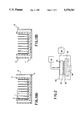
- a plurality of wafers 2 with organic films 1 formed thereon are accommodated in a wafer cassette 3, and this is immersed for a certain period time in a processing tank 5 filled with a processing solution 4 such as a mixed solution of sulfuric acid and hydrogen peroxide. Then, the wafer cassette 3 is immersed in a rinse tank 6 with ultra pure water to remove any chemical solution attached on the substrate or residue of the photo resist film.
- a processing solution 4 such as a mixed solution of sulfuric acid and hydrogen peroxide.
- a method has been proposed in the Japanese Patent Publication No. 52-12063, by which ozone is supplied to sulfuric acid to remove the photo resist film in order to obtain the same effect without processing of waste solution with its removing ability or without the procedure to replenish the solution.
- the sulfuric acid used for the processing of the photo resist film has a high concentration, and the ratio of water in the procesing solution of the photo resist film is low.
- ozone with lower solubility in sulfuric acid is introduced into the sulfuric acid containing lower ratio of water, ozone is less dissolved into the processing solution.
- the introduction of ozone into the processing solution does not necessarily result in effective use of ozone. Accordingly, even when ozone is introduced into sulfuric acid, the oxidizing ability of ozone is not effectively utilized.
- a typical dry method for removing photo resist film is a method using oxygen plasma. According to this method, oxygen plasma is generated by high frequency energy to oxidize the photo resist film and provides a high oxidizing ability. However, during generation of the plasma, high energy charged particles and ions are generated, and the dielectric breakdown or property of the semiconductor device to be manufactured is impaired, and there is now strong demand on a dry method for removing photo resist without such problems.
- FIG. 2 shows the dry method for removing the organic substance by ozone.
- a wafer 22 such as silicon, where an organic film 21 is formed, is placed on a substrate stage 25 kept at 200° C. to 300° C. by a heating device 24 in a processing unit 23, and a gas containing a high concentration of ozone generated by an ozone generator 27 is injected on the organic film through injection nozzles 26 mounted on upper portion of the processing unit, and the organic film is removed by ozone.
- the substrate stage 25 is rotated.
- the portions for introducing and injecting ozone are cooled down so that a high concentration ozone can be introduced into the processing unit.
- an ozone decomposing unit 28 is provided to decompose ozone remaining in the gas, which is discharged from the processing unit.
- the dry processing by ozone is a very effective method which can be conducted without damaging the semiconductor device, and it is possible to remove the photo resist film by the processing using ozone in the case of a normal photo resist film.
- ozone when reactive ion etching is performed or when doping of impurities such as arsenic is carried out at high concentration by ion implantation, the photo resist film is not completely removed and a residue may remain.
- the processing by plasma for long time may adversely affect the semiconductor device, and there is a problem in processing by oxygen plasma for long period when of an organic film with high ion implantation and with high tolerance to oxygen plasma.
- a photo resist film is processed by immersing it in a mixed solution containing sulfuric acid and hydrogen peroxide according to a normal wet method for removing photo resist film, or by a dry processing using ozone or oxygen plasma performed at relatively low temperature and in relatively short time without impairing semiconductor device.
- a substrate such as silicon, from which an organic substance is not completely removed, is rinsed by ultra pure water containing ozone in dissolved state or in bubbling state (hereinafter referred as "solution containing ozone).
- solution containing ozone ultra pure water containing ozone in dissolved state or in bubbling state
- FIG. 1 shows a process for removing an organic film by a wet method
- FIG. 2 shows a process for removing an organic substance by a dry method using ozone
- FIG. 3 represents a process for removal by ultra pure water containing ozone after a wet processing using an oxidizing agent of the present invention.
- FIG. 4 shows a process for removal by ultra pure water containing ozone after a dry processing of an organic substance using ozone according to the present invention.
- a photo resist film is processed by immersing it in a mixed solution of sulfuric acid and hydrogen peroxide by a normal wet method for removing photo resist film, or a dry processing using oxygen plasma is performed at relatively low temperature and in relatively short time without impairing semiconductor device. Then, a substrate such as silicon, from which an organic substance is not completely removed, is rinsed by a solution containing ozone in dissolved state or in bubbling state (a solution containing ozone), prepared by introducing ozone into ultra pure water.
- a photo resist film after ion implantation with residue attached on it, not removable by normal wet type processing or by processing using ozone can be completely removed.
- the processing by ozone is performed by processed water which is prepared by supplying a gas containing ozone into ultra pure water.
- processed water which is prepared by supplying a gas containing ozone into ultra pure water.
- gaseous ozone obtained from a silent discharge type generator, but also high concentration ozone water, obtained by an electrolysis unit for water, are used, in which high concentration ozone water prepared by dissolving gaseous ozone in ultra pure water in advance or a lead dioxide electrode as anode and a cation exchange membrane of fluororesin type is used as solid macromolecular electrolyte.
- the photo resist film is oxidized and decomposed in the processing using ozone by the strong oxidizing action of oxygen generated when ozone is decomposed, it is possible to promote the processing of injecting ozone by increasing the temperature of ultra pure water in a processing tank by ozone. In this case, it is preferable to maintain the temperature in the ozone processing tank at 40° C. to 100° C.
- a porous plate made of glass, ceramics, etc. with many fine pores may be provided on a portion to introduce ozone into the ultra pure water.
- the concentration of ozone in the gas containing ozone to be supplied to the ozone-processing tank is at least about 10,000 ppm or more, more preferably at least about 25,000 ppm or more, most preferably at least about 50,000 ppm ozone or more.
- ozone-containing gas in a bubble state or form reaches and contacts the organic film on the substrates in an ozone-processing tank, and provides an extensive effect for removing the organic film by acting on the organic film in that state in the presence of water.
- the ozone-containing gas in an ozone-processing tank where bubbles of ozone-containing gas do not exist, if the processed water is heated to an elevated temperature, the ozone cannot remain dissolved in the processed water since the ozone is immediately decomposed, and thus sufficient effect on an organic film by the ozone cannot be obtained.
- the ozone-containing gas in the method of the present invention where an ozone-containing gas in a bubble state is brought to act on the organic film on the substrate, the ozone-containing gas can act on the organic film when the ultra pure water is heated in the ozone-processing tank, and a very high effect on the film can be obtained.
- ozone has very high oxidizing effect and adversely affects human body, it is necessary to decompose ozone to oxygen by providing an ozone decomposing unit to decompose the discharged ozone from the ozone processing tank.
- FIG. 3 shows an apparatus to be used for a method for removing a photo resist film in ultra pure water containing ozone after the photo resist film has been processed by a chemical solution.
- a plurality of substrates 32, on which photo resist films 31 are formed are accommodated in a cassette 33.
- This cassette 33 is immersed for a certain period of time in a wet processing tank 4, which is filled with a processing solution such as a mixed solution of sulfuric acid and hydrogen peroxide, and the photo resist films are removed by a wet method. Then, the cassette is immersed in an ozone processing tank 35 shown in FIG. 3 (B) and is processed.
- a processing solution such as a mixed solution of sulfuric acid and hydrogen peroxide
- the ozone processing tank comprises a supply pipe 36 for ultra pure water, an ozone supply pipe 38 for supplying ozone generated in an ozone generator 37, and a solution discharge pipe 39.
- the temperature of the solution in the ozone processing tank is adjusted to a desired value by a heater 40 and a temperature regulator 41.
- an ozone decomposing unit 42 is provided, and the discharge of ozone to the working environment is prevented.
- FIG. 4 shows a method for processing photo resist films in ultra pure water containing ozone by injecting ozone after the films have been processed by a dry processing using ozone.
- a substrate 52 with photo resist film 51 formed on it is placed on a substrate stage 54 in a processing chamber 53.
- the substrate stage 54 is rotatable by a rotating mechanism 55, and a heating element 56 is furnished in the substrate stage, and the temperature is maintained at a predetermined value by a temperature controller 57.
- a gas containing ozone is generated in an ozone generator 58 and is injected through a plurality of injection nozzles 59, placed face-to-face to the substrate, toward the surface of the substrate.
- a channel toward the processing chamber and the injection nozzles are cooled by a cooling medium 60 so that the gas containing a high concentration ozone can reach the substrate surface uniformly.
- the ozone decomposing unit 61 which comprises an ozone decomposing heater or an ozone decomposing catalyst.
- the processing speed can be substantially increased by furnishing a plurality of processing chambers in a dry processing unit using ozone.
- the substrate 52 is housed in a cassette 62 as shown in FIG. 4 (B) just as in the case of the substrate after the completion of processing by chemical solution.
- the cassette 62 is then immersed in an ozone processing tank 63, and the residue is removed by water containing ozone.
- the ozone processing tank comprises an ultra pure water supply pipe 64, an ozone supply pipe 66 for supplying ozone generated in an ozone generator 65, and a solution discharge pipe 67.
- the temperature of the solution in the ozone processing tank is regulated to a predetermined value by a heater 68 and a temperature regulator 69.
- An ozone decomposing unit 70 is furnished to prevent the contamination of the working environment by ozone discharged from the ozone processing tank.
- the removal of photo resist film is not performed uniformly from the wafer Surface but it is influenced by a pattern formed on the photo resist surface.
- the present inventors studied a method to evaluate the removal of photo resist film and evaluated it by the following method.
- the mode of detachment differs according to form, line width, area, etc., and the larger the line width or the area is, the more rarely the detachment occurs.
- the pattern was divided into four parts for observation: portion with identification symbol, pad portion, lead portion and wiring portion, with difficulty of detachment in this order.
- the wiring portion was divided into wiring top and a portion around wiring for observation.
- Table 1 A photo resist film completely detached is represented by o, a photo resist film partially remaining is shown by ⁇ , and a photo resist film not removed is shown by x. Comparison was also made by numerical values with complete removal as 100.
- a silicon wafer of 150 mm in diameter positive type photo resist (OFPR-800; Tokyo Ohka Kogyo Co., Ltd.) was coated in thickness of 1.5 ⁇ m, and exposure and development were performed. Then, ion implantation was performed with arsenic at concentration of 1 ⁇ 10 15 /cm 2 to 4 ⁇ 10 15 /cm 2 .
- the wafer was placed on a substrate stage in a dry ozone processing unit. With the substrate stage maintained at 300° C., oxygen containing ozone at concentration of 60,000 ppm was supplied from injection nozzles at a flow rate of 10 liters/min. for 2 minutes.
- Ion implantation was performed by the same procedure as in the Example 5 on a silicon wafer with arsenic at concentration of 3 ⁇ 10 15 /cm 2 and 4 ⁇ 10 15 /cm 2 , and the wafer was immersed for 5 minutes in a processing solution containing sulfuric acid of 90% concentration and hydrogen peroxide of 35% concentration mixed at a ratio of 4:1. Then, the wafer was immersed in an ozone processing solution of ultra pure water containing ozone for 5 minutes when the arsenic concentration was 3 ⁇ 10 15 /cm 2 and for 6 minutes when the arsenic concentration was 4 ⁇ 10 15 /cm 2 and this was rinsed for 5 minutes under running ultra pure water.
- the method for processing an organic film according to the present invention it is possible to completely remove a photo resist film, which has been deteriorated by high concentration ion implantation or by reactive ion etching and which has been difficult in the past to remove by a dry type processing to remove organic film or by a wet type processing using a solution containing sulfuric acid and hydrogen peroxide. This makes it possible to shorten the manufacturing process and to reduce percent defective in the manufacture of semiconductor devices.
Abstract
The method for removing organic film according to the present invention is very effective for removing a photo resist film in a process for manufacturing semiconductor device. A substrate (32) having a photo resist film (31) formed on it is processed in a wet processing tank (34) filled with a processing solution such as a mixed solution containing sulfuric acid and hydrogen peroxide or by a dry processing using oxygen plasma. Then, it is processed in an ozone processing tank (34) filled with a solution where ozone or ozone water has been infused, and the organic film is removed.
Description
This application is a continuation-in-part of application Ser. No. 07/853,702 filed Jun. 8, 1992, now abandoned.
The present invention relates to a method for removing an organic film, and in particular to a method for removing a photo resist film, i.e. an organic macromolecular compound used in manufacture of semiconductor device by photolithography, without damaging the semiconductor device.
In a process for manufacturing a semiconductor device such as IC, LSI, etc., an organic photosensitive macromolecular compound is coated on a semiconductor substrate such as silicon or a glass substrate in order to form a fine electric element or circuit, and the compound is exposed to ionizing radiation such an ultraviolet ray through a photo mask where a pattern such as a predetermined circuit is formed. Then, the photo resist is developed, and a positive or negative circuit pattern is prepared on the photo resist on the substrate, and a film is formed on a substrate without the photo resist by CVD, sputtering, etc. Alternatively, chemical etching, RIE (reactive ion etching), diffusion by heating impurity element, or ion implantation are performed. After a series of processings are completed, the film of photo resist on the substrate is removed by chemical processing. In a process for manufacturing IC and LSI, after various processings by coating such photo resist, the photo resist film is removed not only by a single procedure but by several procedures.
To remove the photo resist film, various methods are adopted, and it is necessary to completely remove the photo resist film because the subsequent processes may be affected adversely if the removal of the photo resist is incomplete. Particularly, since the line width of a circuit of a semiconductor device to be formed is finer because of the introduction of higher integration of the semiconductor device in recent years, the influence of residue of the photo resist film becomes larger than is the case with lower integration, and it is necessary to remove it completely.
Various methods are employed for the removal of the photo resist film including a wet method using a chemical solution and a dry method using oxygen plasma.
In the wet method for removing photo resist film, sulfuric acid is normally used, and it is general practice to mix the acid with hydrogen peroxide to increase oxidizing ability of the sulfuric acid.
When the photo resist film is removed using a mixed solution of sulfuric acid and hydrogen peroxide, a chemical solution such as sulfuric acid attached on the film is removed after the removal of the photo resist film, and ultra pure water is used for removing and cleaning the residue.
As is shown in FIG. 1(A), to remove an organic film by a normal wet method, a plurality of wafers 2 with organic films 1 formed thereon are accommodated in a wafer cassette 3, and this is immersed for a certain period time in a processing tank 5 filled with a processing solution 4 such as a mixed solution of sulfuric acid and hydrogen peroxide. Then, the wafer cassette 3 is immersed in a rinse tank 6 with ultra pure water to remove any chemical solution attached on the substrate or residue of the photo resist film. There are many types of rinse tanks, while an overflow type tank is widely used and the rinse tank is provided with an ultra pure water inlet 7 and an outlet 8 for the solution.
In the removal of the photo resist film by the mixed solution of sulfuric acid and hydrogen peroxide, oxidizing decomposition of the photo resist film by oxygen generated through decomposition of hydrogen peroxide plays an important role. To maintain the oxidizing ability of this mxied solution, it is necessary to replenish a new solution by removing sulfuric acid and hydrogen peroxide, which have been consumed by oxidizing decomposition of the photo resist film and have decreased concentration.
A method has been proposed in the Japanese Patent Publication No. 52-12063, by which ozone is supplied to sulfuric acid to remove the photo resist film in order to obtain the same effect without processing of waste solution with its removing ability or without the procedure to replenish the solution.
In the case of a normal photo resist film, it is possible to remove the photo resist film by the introduction of ozone into the sulfuric acid as described above. In some cases, however, when reactive ion etching is performed or high concentration arsenic is used by ion implatation for doping of impurities into the semiconductor, the photo resist film is not removed completely and a residue remains. When high energy ions are used in an ion implantation method, arsenic and others used in the ion implantation may chemically react with the photo resist, and the photo resist film maybe converted into a substance which is not easily oxidized. As a result, oxidizing decomposition is prevented because of the processing solution.
The sulfuric acid used for the processing of the photo resist film has a high concentration, and the ratio of water in the procesing solution of the photo resist film is low. When ozone with lower solubility in sulfuric acid is introduced into the sulfuric acid containing lower ratio of water, ozone is less dissolved into the processing solution. Thus, the introduction of ozone into the processing solution does not necessarily result in effective use of ozone. Accordingly, even when ozone is introduced into sulfuric acid, the oxidizing ability of ozone is not effectively utilized.
On the other hand, in the processing by a chemical solution containing sulfuric acid and hydrogen peroxide or chemical solution with dissolved ozone, various facilities for introducing the chemical solution are required, and also facilities for the processing waste solution are needed. Further, it is necessary to provide a process to remove the chemical solution by completely rinsing with ultra pure water after the processing with the chemical solution.
Under such circumstances, the dry method for processing is now more frequently used instead of the wet processing method using a chemical solution. A typical dry method for removing photo resist film is a method using oxygen plasma. According to this method, oxygen plasma is generated by high frequency energy to oxidize the photo resist film and provides a high oxidizing ability. However, during generation of the plasma, high energy charged particles and ions are generated, and the dielectric breakdown or property of the semiconductor device to be manufactured is impaired, and there is now strong demand on a dry method for removing photo resist without such problems.
To overcome these difficulties, a method is now adopted to separate the plasma generator from the processing unit to remove the organic substance. There is another dry method is adopted to remove the organic film using ozone, which has high oxidizing ability next to fluorine.
FIG. 2 shows the dry method for removing the organic substance by ozone. A wafer 22 such as silicon, where an organic film 21 is formed, is placed on a substrate stage 25 kept at 200° C. to 300° C. by a heating device 24 in a processing unit 23, and a gas containing a high concentration of ozone generated by an ozone generator 27 is injected on the organic film through injection nozzles 26 mounted on upper portion of the processing unit, and the organic film is removed by ozone. To attain uniform processing of the organic film, the substrate stage 25 is rotated. To effectively utilize ozone, which is vulnerable to thermal decomposition, the portions for introducing and injecting ozone are cooled down so that a high concentration ozone can be introduced into the processing unit. To decompose ozone remaining in the gas, which is discharged from the processing unit, an ozone decomposing unit 28 is provided.
The dry processing by ozone is a very effective method which can be conducted without damaging the semiconductor device, and it is possible to remove the photo resist film by the processing using ozone in the case of a normal photo resist film. However, when reactive ion etching is performed or when doping of impurities such as arsenic is carried out at high concentration by ion implantation, the photo resist film is not completely removed and a residue may remain.
Even in such case, it is possible to accomplish the processing by increasing the heating temperature of the substrate stage of the processing unit. However metal such aluminum used in the semiconductor device may undergo unnecessary diffusion by heat and the property of the semiconductor device may be deteriorated. Thus, there is also a problem in the processing at high temperature.
In removing the organic film by oxygen plasma, the processing by plasma for long time may adversely affect the semiconductor device, and there is a problem in processing by oxygen plasma for long period when of an organic film with high ion implantation and with high tolerance to oxygen plasma.
It is therefore an object of the present invention to provide a method, by which it is possible to remove a photo resist film, which is difficult to remove by a wet method using chemical solution, and also to remove a photo resist film, which is deteriorated by ion implantation and is difficult to remove without processing at a high temperature for long time by a dry method, by a processing conducted at a relatively low temperature within a short time and without impairing the semiconductor device.
A photo resist film is processed by immersing it in a mixed solution containing sulfuric acid and hydrogen peroxide according to a normal wet method for removing photo resist film, or by a dry processing using ozone or oxygen plasma performed at relatively low temperature and in relatively short time without impairing semiconductor device. A substrate such as silicon, from which an organic substance is not completely removed, is rinsed by ultra pure water containing ozone in dissolved state or in bubbling state (hereinafter referred as "solution containing ozone). Thus, a photo resist film after ion implantation with residue attached on it, not removable by normal wet type processing or by processing using ozone, can be completely removed.
FIG. 1 shows a process for removing an organic film by a wet method;
FIG. 2 shows a process for removing an organic substance by a dry method using ozone;
FIG. 3 represents a process for removal by ultra pure water containing ozone after a wet processing using an oxidizing agent of the present invention; and
FIG. 4 shows a process for removal by ultra pure water containing ozone after a dry processing of an organic substance using ozone according to the present invention.
According to the present invention, a photo resist film is processed by immersing it in a mixed solution of sulfuric acid and hydrogen peroxide by a normal wet method for removing photo resist film, or a dry processing using oxygen plasma is performed at relatively low temperature and in relatively short time without impairing semiconductor device. Then, a substrate such as silicon, from which an organic substance is not completely removed, is rinsed by a solution containing ozone in dissolved state or in bubbling state (a solution containing ozone), prepared by introducing ozone into ultra pure water. As the result, a photo resist film after ion implantation with residue attached on it, not removable by normal wet type processing or by processing using ozone, can be completely removed.
The processing by ozone is performed by processed water which is prepared by supplying a gas containing ozone into ultra pure water. In supplying ozone into the ultra pure water, not only gaseous ozone obtained from a silent discharge type generator, but also high concentration ozone water, obtained by an electrolysis unit for water, are used, in which high concentration ozone water prepared by dissolving gaseous ozone in ultra pure water in advance or a lead dioxide electrode as anode and a cation exchange membrane of fluororesin type is used as solid macromolecular electrolyte.
To obtain a high concentration ozone in a silent discharge type ozone generator, it is desirable to supply a gas with high oxygen concentration such as pure oxygen to the ozone generator.
Because the photo resist film is oxidized and decomposed in the processing using ozone by the strong oxidizing action of oxygen generated when ozone is decomposed, it is possible to promote the processing of injecting ozone by increasing the temperature of ultra pure water in a processing tank by ozone. In this case, it is preferable to maintain the temperature in the ozone processing tank at 40° C. to 100° C.
If the concentration of the gas containing ozone to be supplied into the ozone processing tank is a higher, higher rinsing effect can be obtained. A porous plate made of glass, ceramics, etc. with many fine pores may be provided on a portion to introduce ozone into the ultra pure water. Thus, it is possible to promote the processing by ozone by promoting of dissolution of the gas containing ozone into the ultra pure water by increasing the contact with the ultra pure water through the formation of fine bubbles by the porous plate. It is preferable that the concentration of ozone in the gas containing ozone to be supplied to the ozone-processing tank is at least about 10,000 ppm or more, more preferably at least about 25,000 ppm or more, most preferably at least about 50,000 ppm ozone or more. In the method for removing organic substances of the present invention, ozone-containing gas in a bubble state or form reaches and contacts the organic film on the substrates in an ozone-processing tank, and provides an extensive effect for removing the organic film by acting on the organic film in that state in the presence of water.
In an ozone-processing tank where bubbles of ozone-containing gas do not exist, if the processed water is heated to an elevated temperature, the ozone cannot remain dissolved in the processed water since the ozone is immediately decomposed, and thus sufficient effect on an organic film by the ozone cannot be obtained. However, in the method of the present invention where an ozone-containing gas in a bubble state is brought to act on the organic film on the substrate, the ozone-containing gas can act on the organic film when the ultra pure water is heated in the ozone-processing tank, and a very high effect on the film can be obtained.
Because ozone has very high oxidizing effect and adversely affects human body, it is necessary to decompose ozone to oxygen by providing an ozone decomposing unit to decompose the discharged ozone from the ozone processing tank.
By the method of the present invention, it is possible to remove the photo resist film of both positive and negative types.
In the following, description will be given on the present invention, with reference to the drawings.
FIG. 3 shows an apparatus to be used for a method for removing a photo resist film in ultra pure water containing ozone after the photo resist film has been processed by a chemical solution. As shown in FIG. 3 (A), a plurality of substrates 32, on which photo resist films 31 are formed, are accommodated in a cassette 33. This cassette 33 is immersed for a certain period of time in a wet processing tank 4, which is filled with a processing solution such as a mixed solution of sulfuric acid and hydrogen peroxide, and the photo resist films are removed by a wet method. Then, the cassette is immersed in an ozone processing tank 35 shown in FIG. 3 (B) and is processed. The ozone processing tank comprises a supply pipe 36 for ultra pure water, an ozone supply pipe 38 for supplying ozone generated in an ozone generator 37, and a solution discharge pipe 39. The temperature of the solution in the ozone processing tank is adjusted to a desired value by a heater 40 and a temperature regulator 41.
To prevent the contamination of the working environment by ozone discharged from the ozone processing tank, an ozone decomposing unit 42 is provided, and the discharge of ozone to the working environment is prevented.
FIG. 4 shows a method for processing photo resist films in ultra pure water containing ozone by injecting ozone after the films have been processed by a dry processing using ozone.
As shown in FIG. 4 (A), a substrate 52 with photo resist film 51 formed on it is placed on a substrate stage 54 in a processing chamber 53. The substrate stage 54 is rotatable by a rotating mechanism 55, and a heating element 56 is furnished in the substrate stage, and the temperature is maintained at a predetermined value by a temperature controller 57.
A gas containing ozone is generated in an ozone generator 58 and is injected through a plurality of injection nozzles 59, placed face-to-face to the substrate, toward the surface of the substrate. To prevent decomposition of the gas containing ozone by heat, a channel toward the processing chamber and the injection nozzles are cooled by a cooling medium 60 so that the gas containing a high concentration ozone can reach the substrate surface uniformly.
In the gas discharged from the ozone processing chamber, unreacted ozone remains together with carbon dioxide generated by decomposed organic substances and water, and this gas cannot be discharged. Thus, it is necessary to discharge the gas after ozone has been completely decomposed by the ozone decomposing unit 61, which comprises an ozone decomposing heater or an ozone decomposing catalyst.
In case the dry processing using ozone is performed by a leaf type processing as in the present embodiment, the processing speed can be substantially increased by furnishing a plurality of processing chambers in a dry processing unit using ozone.
After the processing by ozone has been completed, the substrate 52 is housed in a cassette 62 as shown in FIG. 4 (B) just as in the case of the substrate after the completion of processing by chemical solution. The cassette 62 is then immersed in an ozone processing tank 63, and the residue is removed by water containing ozone.
The ozone processing tank comprises an ultra pure water supply pipe 64, an ozone supply pipe 66 for supplying ozone generated in an ozone generator 65, and a solution discharge pipe 67. The temperature of the solution in the ozone processing tank is regulated to a predetermined value by a heater 68 and a temperature regulator 69.
It is preferable to provide an inlet for the supply pipe 64 of ultra pure water on the lower portion of the ozone processing tank and to provide the solution discharge pipe on the upper portion of the ozone processing tank so that the solution is discharged by overflow.
An ozone decomposing unit 70 is furnished to prevent the contamination of the working environment by ozone discharged from the ozone processing tank.
In the following, the features of the invention will be described referring to several examples.
On a silicon wafer of 150 mm in diameter, positive type photo resist (OFPR-800; Tokyo Ohka Kogyo Co., Ltd.) was coated in a thickness of 1.5 μm, and exposure and development were performed. Then, ion implantation was carried out with arsenic at concentration of 1×10¹⁵ /cm2 to 3×10¹⁵ /cm2. The wafer was immersed for 5 minutes in a processing solution which contained sulfuric acid of 90% concentration and hydrogen peroxide of 35% concentration mixed at a ratio of 4:1. Further, the wafer was immersed for 5 minutes at room temperature in ultra pure water with gas containing varying concentrations of ozone and is then rinsed in running ultra pure water.
The removal of photo resist film is not performed uniformly from the wafer Surface but it is influenced by a pattern formed on the photo resist surface. The present inventors studied a method to evaluate the removal of photo resist film and evaluated it by the following method.
The mode of detachment differs according to form, line width, area, etc., and the larger the line width or the area is, the more rarely the detachment occurs. Thus, the pattern was divided into four parts for observation: portion with identification symbol, pad portion, lead portion and wiring portion, with difficulty of detachment in this order. Then, the wiring portion was divided into wiring top and a portion around wiring for observation. The results are summarized in Table 1. A photo resist film completely detached is represented by o, a photo resist film partially remaining is shown by Δ, and a photo resist film not removed is shown by x. Comparison was also made by numerical values with complete removal as 100.
              TABLE 1
______________________________________
Arsenic                                  Overall
infusion
        Ozone   Identifi-                evaluation
conc.   conc.   cation                   of
(cm.sup.-2)
        (ppm)   symbol   Pad  Lead Wiring
                                         detachment
______________________________________
1 × 10.sup.15
        95000   o        o    o    o     100
1 × 10.sup.15
        57000   o        o    o    o     100
1 × 10.sup.15
        41700   o        o    o    o     100
2 × 10.sup.15
        95000   o        o    o    o     100
2 × 10.sup.15
        57000   o        o    o    o     100
2 × 10.sup.15
        41700   Δ  Δ
                              Δ
                                   o      65
3 × 10.sup.15
        95000   o        o    o    o     100
3 × 10.sup.15
        57000   Δ  Δ
                              Δ
                                   o      65
3 × 10.sup.15
        41700   Δ  Δ
                              Δ
                                   o      65
______________________________________
Instead of the gas containing ozone supplied to the ozone processing tank, ultra pure water with dissolved ozone was used, and the same processing as in the Example 1 was performed. This was evaluated by the same method as in the Example 1 and the results are shown in Table 2. The ozone concentration in ultra pure water was expressed as ozone water concentration in Table 2.
              TABLE 2
______________________________________
Arsenic Ozone                            Overall
infusion
        water   Identifi-                evaluation
conc.   conc.   cation                   of
(cm.sup.-2)
        (ppm)   symbol   Pad  Lead Wiring
                                         detachment
______________________________________
1 × 10.sup.15
        21.8    o        o    o    o     100
2 × 10.sup.15
        23.9    o        o    o    o     100
3 × 10.sup.15
        23.3    Δ  o    o    o      95
______________________________________
By varying the temperature of ultra pure water in the ozone processing tank, processing was performed by the same procedure as in the Example 1 except that the gas containing ozone was injected. The results are summarized in Table 3.
              TABLE 3
______________________________________
       Liquid                               Overall
Arsenic
       tem-            Identi-              evalua-
infusion
       per-    Ozone   fica-                tion of
conc.  ature   conc.   tion            Wir- detach-
(cm.sup.-2)
       (°C.)
               (ppm)   symbol
                             Pad  Lead ing  ment
______________________________________
3 × 10.sup.15
        25     57000   Δ
                             Δ
                                  Δ
                                       o     65
3 × 10.sup.15
        35     57000   Δ
                             Δ
                                  Δ
                                       o     65
3 × 10.sup.15
        50     57000   Δ
                             o    o    o     95
3 × 10.sup.15
       100     57000   o     o    o    o    100
______________________________________
The processing was performed only by the mixed solution of sulfuric acid and hydrogen peroxide and not by ozone, and the removal of the photo resist was evaluated by the same method as in the Example 1. The results are shown in Table 4.
              TABLE 4
______________________________________
Arsenic                               Overall
infusion Identification               evaluation of
conc. (cm.sup.-2)
         symbol     Pad    Lead Wiring
                                      detachment
______________________________________
1 × 10.sup.15
         o          o      o    o     100
1 × 10.sup.15
         o          o      o    o     100
2 × 10.sup.15
         Δ    Δ
                           Δ
                                Δ
                                      100
2 × 10.sup.15
         Δ    Δ
                           Δ
                                o     100
3 × 10.sup.15
         Δ    Δ
                           Δ
                                o     100
3 × 10.sup.15
         Δ    Δ
                           Δ
                                o      65
3 × 10.sup.15
         Δ    Δ
                           Δ
                                o      65
______________________________________
On a silicon wafer of 150 mm in diameter, positive type photo resist (OFPR-800; Tokyo Ohka Kogyo Co., Ltd.) was coated in thickness of 1.5 μm, and exposure and development were performed. Then, ion implantation was performed with arsenic at concentration of 1×10¹⁵ /cm2 to 4×10¹⁵ /cm2. The wafer was placed on a substrate stage in a dry ozone processing unit. With the substrate stage maintained at 300° C., oxygen containing ozone at concentration of 60,000 ppm was supplied from injection nozzles at a flow rate of 10 liters/min. for 2 minutes.
In the ozone processing tank with the gas containing ozone at concentration of 95,000 ppm in ultra pure water, rinsing was performed for 5 minutes when arsenic concentration was 3×10¹⁵ /cm2, and for 6 minutes when it was 4×10¹⁵ /cm2. This was evaluated by the same procedure as in the Example 1, and the results are shown in Table 5.
              TABLE 5
______________________________________
       Liquid                               Overall
Arsenic
       tem-            Identi-              evalua-
infusion
       per-    Ozone   fica-                tion of
conc.  ature   conc.   tion            Wir- detach-
(cm.sup.-2)
       (°C.)
               (ppm)   symbol
                             Pad  Lead ing  ment
______________________________________
1 × 10.sup.15
       25      95000   o     o    o    o    100
2 × 10.sup.15
       25      95000   o     o    o    o    100
3 × 10.sup.15
       25      95000   o     o    o    o    100
4 × 10.sup.15
       25      95000   o     o    o    o    100
______________________________________
Ion implantation was performed by the same procedure as in the Example 5 on a silicon wafer with arsenic at concentration of 3×10¹⁵ /cm2 and 4×10¹⁵ /cm2, and the wafer was immersed for 5 minutes in a processing solution containing sulfuric acid of 90% concentration and hydrogen peroxide of 35% concentration mixed at a ratio of 4:1. Then, the wafer was immersed in an ozone processing solution of ultra pure water containing ozone for 5 minutes when the arsenic concentration was 3×10¹⁵ /cm2 and for 6 minutes when the arsenic concentration was 4×10¹⁵ /cm2 and this was rinsed for 5 minutes under running ultra pure water.
The removal of the photo resist was evaluated by the same procedure as in the Example 5, and the results are given in Table 6.
              TABLE 6
______________________________________
       Liquid                               Overall
Arsenic
       tem-            Identi-              evalua-
infusion
       per-    Ozone   fica-                tion of
conc.  ature   conc.   tion            Wir- detach-
(cm.sup.-2)
       (°C.)
               (ppm)   symbol
                             Pad  Lead ing  ment
______________________________________
3 × 10.sup.15
       25      95000   o     o    o    o    100
4 × 10.sup.15
       25      95000   Δ
                             Δ
                                  Δ
                                       o     60
______________________________________
By the method for processing an organic film according to the present invention, it is possible to completely remove a photo resist film, which has been deteriorated by high concentration ion implantation or by reactive ion etching and which has been difficult in the past to remove by a dry type processing to remove organic film or by a wet type processing using a solution containing sulfuric acid and hydrogen peroxide. This makes it possible to shorten the manufacturing process and to reduce percent defective in the manufacture of semiconductor devices.
Claims (4)
1. A method for removing an organic film from a substrate, the method comprising removing the organic film by subjecting the film to a gas containing oxygen plasma or ozone in a dry method or to a solution containing an oxidizing agent in a wet method, and thereafter immersing said substrate in an ozone processing tank containing a solution of ozone in ultra pure water, wherein said solution of ozone in ultra pure water is prepared by blowing ozone-containing gas having an ozone content of at least 10,000 ppm through ultra pure water and said ozone-containing gas contacts the organic film on the substrate in the form of gas bubbles.
2. A method for removing an organic film according to claim 1, wherein said oxidizing agent is a mixed solution of sulfuric acid and hydrogen peroxide.
3. A method for removing an organic film according to claim 1, wherein the organic film has been processed by reactive ion etching or ion implantation.
4. A method for removing an organic film according to claim 1, wherein the solution in the ozone processing tank is a heated solution.
Priority Applications (1)
| Application Number | Priority Date | Filing Date | Title |
|---|---|---|---|
| US08/110,646 US5378317A (en) | 1990-10-09 | 1991-10-09 | Method for removing organic film |
Applications Claiming Priority (5)
| Application Number | Priority Date | Filing Date | Title |
|---|---|---|---|
| JP27089890A JP3152430B2 (en) | 1990-10-09 | 1990-10-09 | Organic film removal method |
| JP2-270898 | 1990-10-09 | ||
| PCT/JP1991/001374 WO1992006489A1 (en) | 1990-10-09 | 1991-10-09 | Method of removing organic coating |
| US08/110,646 US5378317A (en) | 1990-10-09 | 1991-10-09 | Method for removing organic film |
| US85370292A | 1992-06-08 | 1992-06-08 |
Related Parent Applications (1)
| Application Number | Title | Priority Date | Filing Date |
|---|---|---|---|
| US85370292A Continuation-In-Part | 1990-10-09 | 1992-06-08 |
Publications (1)
| Publication Number | Publication Date |
|---|---|
| US5378317A true US5378317A (en) | 1995-01-03 |
Family
ID=26549445
Family Applications (1)
| Application Number | Title | Priority Date | Filing Date |
|---|---|---|---|
| US08/110,646 Expired - Fee Related US5378317A (en) | 1990-10-09 | 1991-10-09 | Method for removing organic film |
Country Status (1)
| Country | Link |
|---|---|
| US (1) | US5378317A (en) |
Cited By (36)
| Publication number | Priority date | Publication date | Assignee | Title |
|---|---|---|---|---|
| US5665168A (en) * | 1994-08-30 | 1997-09-09 | Shin-Etsu Handotai Co., Ltd. | Method for cleaning semiconductor silicon wafer |
| US5674357A (en) * | 1995-08-30 | 1997-10-07 | Taiwan Semiconductor Manufacturing Company, Ltd. | Semiconductor substrate cleaning process |
| WO1998033208A1 (en) * | 1997-01-22 | 1998-07-30 | Fraunhofer-Gesellschaft zur Förderung der angewandten Forschung e.V. | Method and device for cleaning substrate surfaces |
| DE19801360A1 (en) * | 1998-01-16 | 1999-07-22 | Sez Semiconduct Equip Zubehoer | Method for cleaning, etching, or smoothing semiconductor wafer coated surfaces |
| US5930655A (en) * | 1996-11-08 | 1999-07-27 | International Business Machines Corporation | Fluorine barrier layer between conductor and insulator for degradation prevention |
| US5971368A (en) * | 1997-10-29 | 1999-10-26 | Fsi International, Inc. | System to increase the quantity of dissolved gas in a liquid and to maintain the increased quantity of dissolved gas in the liquid until utilized |
| WO2000070667A1 (en) * | 1999-05-14 | 2000-11-23 | Fsi International, Inc. | Method for treating a substrate with heat sensitive agents |
| EP1070157A1 (en) * | 1998-04-06 | 2001-01-24 | Arch Specialty Chemicals, Inc. | Method for removing photoresist and plasma etch residues |
| KR20010034087A (en) * | 1998-11-13 | 2001-04-25 | 다니구찌 이찌로오 | Method and device for removing photoresist film |
| US6235641B1 (en) | 1998-10-30 | 2001-05-22 | Fsi International Inc. | Method and system to control the concentration of dissolved gas in a liquid |
| US6245155B1 (en) | 1996-09-06 | 2001-06-12 | Arch Specialty Chemicals, Inc. | Method for removing photoresist and plasma etch residues |
| US6267125B1 (en) | 1997-05-09 | 2001-07-31 | Semitool, Inc. | Apparatus and method for processing the surface of a workpiece with ozone |
| US6274506B1 (en) | 1999-05-14 | 2001-08-14 | Fsi International, Inc. | Apparatus and method for dispensing processing fluid toward a substrate surface |
| US20020011257A1 (en) * | 1997-02-14 | 2002-01-31 | Degendt Stefan | Method for removing organic contaminants from a semiconductor surface |
| US20020115024A1 (en) * | 1998-11-12 | 2002-08-22 | Mitsubishi Denki Kabushiki Kaisha | Apparatus for removing photoresist film |
| US20020157686A1 (en) * | 1997-05-09 | 2002-10-31 | Semitool, Inc. | Process and apparatus for treating a workpiece such as a semiconductor wafer |
| US6551409B1 (en) * | 1997-02-14 | 2003-04-22 | Interuniversitair Microelektronica Centrum, Vzw | Method for removing organic contaminants from a semiconductor surface |
| US6558477B1 (en) | 2000-10-16 | 2003-05-06 | Micron Technology, Inc. | Removal of photoresist through the use of hot deionized water bath, water vapor and ozone gas |
| US6559064B1 (en) * | 1999-06-04 | 2003-05-06 | Nec Electronics Corporation | Method and apparatus for removing photoresist on semiconductor wafer |
| US20030136429A1 (en) * | 2002-01-22 | 2003-07-24 | Semitool, Inc. | Vapor cleaning and liquid rinsing process vessel |
| US20030205240A1 (en) * | 1997-05-09 | 2003-11-06 | Semitool, Inc. | Apparatus for treating a workpiece with steam and ozone |
| US20040012363A1 (en) * | 2002-03-20 | 2004-01-22 | Fsi International, Inc. | Systems and methods incorporating an end effector with a rotatable and/or pivotable body and/or an optical sensor having a light path that extends along a length of the end effector |
| US20040020513A1 (en) * | 1997-05-09 | 2004-02-05 | Semitool, Inc. | Methods of thinning a silicon wafer using HF and ozone |
| US20040040934A1 (en) * | 2002-09-04 | 2004-03-04 | Tai Chen Chung | Method of etching a photoresist layer disposed on a semiconductor substrate |
| US20040061235A1 (en) * | 1999-12-20 | 2004-04-01 | Barth Edward P. | Dual damascene interconnect structure using low stress fluorosilicate insulator with copper conductors |
| US20040069320A1 (en) * | 1997-05-09 | 2004-04-15 | Semitool, Inc. | Methods for cleaning semiconductor surfaces |
| US6790783B1 (en) * | 1999-05-27 | 2004-09-14 | Micron Technology, Inc. | Semiconductor fabrication apparatus |
| US20040216763A1 (en) * | 1997-05-09 | 2004-11-04 | Semitool, Inc. | Process and apparatus for treating a workpiece using ozone |
| US20040221877A1 (en) * | 1997-05-09 | 2004-11-11 | Semitool, Inc. | Process and apparatus for treating a workpiece with gases |
| US20050034745A1 (en) * | 1997-05-09 | 2005-02-17 | Semitool, Inc. | Processing a workpiece with ozone and a halogenated additive |
| US20050101144A1 (en) * | 2003-11-07 | 2005-05-12 | Industrial Technology Research Institute | Method and apparatus for treating a substrate surface by bubbling |
| US20050133067A1 (en) * | 1997-05-09 | 2005-06-23 | Bergman Eric J. | Processing a workpiece using water, a base, and ozone |
| US20050215063A1 (en) * | 1997-05-09 | 2005-09-29 | Bergman Eric J | System and methods for etching a silicon wafer using HF and ozone |
| US20050236363A1 (en) * | 1997-05-09 | 2005-10-27 | Bergman Eric J | System and methods for polishing a wafer |
| US20070259527A1 (en) * | 2006-05-08 | 2007-11-08 | Pei-Yu Chou | Automatic process control of after-etch-inspection critical dimension |
| US20110100796A1 (en) * | 2009-10-30 | 2011-05-05 | Industrial Technology Research Institute | System and method for producing supercritical ozone |
Citations (9)
| Publication number | Priority date | Publication date | Assignee | Title |
|---|---|---|---|---|
| US4006040A (en) * | 1975-12-31 | 1977-02-01 | General Electric Company | Semiconductor device manufacture |
| US4519846A (en) * | 1984-03-08 | 1985-05-28 | Seiichiro Aigo | Process for washing and drying a semiconductor element |
| JPS62213127A (en) * | 1986-03-13 | 1987-09-19 | Nec Corp | Semiconductor wafer washing equipment |
| US4749640A (en) * | 1986-09-02 | 1988-06-07 | Monsanto Company | Integrated circuit manufacturing process |
| JPS648630A (en) * | 1986-09-22 | 1989-01-12 | Tokyo Electron Ltd | Cleaning method |
| JPS6476726A (en) * | 1987-09-17 | 1989-03-22 | Hitachi Ltd | Manufacture of semiconductor |
| US4938839A (en) * | 1986-02-14 | 1990-07-03 | Fujitsu Limited | Method of removing photoresist on a semiconductor wafer |
| US5049519A (en) * | 1985-09-16 | 1991-09-17 | Texas Instruments Incorporated | Latch-up resistant CMOS process |
| US5102629A (en) * | 1987-07-23 | 1992-04-07 | Asahi Glass Company, Ltd. | Field formation apparatus |
-
1991
- 1991-10-09 US US08/110,646 patent/US5378317A/en not_active Expired - Fee Related
Patent Citations (9)
| Publication number | Priority date | Publication date | Assignee | Title |
|---|---|---|---|---|
| US4006040A (en) * | 1975-12-31 | 1977-02-01 | General Electric Company | Semiconductor device manufacture |
| US4519846A (en) * | 1984-03-08 | 1985-05-28 | Seiichiro Aigo | Process for washing and drying a semiconductor element |
| US5049519A (en) * | 1985-09-16 | 1991-09-17 | Texas Instruments Incorporated | Latch-up resistant CMOS process |
| US4938839A (en) * | 1986-02-14 | 1990-07-03 | Fujitsu Limited | Method of removing photoresist on a semiconductor wafer |
| JPS62213127A (en) * | 1986-03-13 | 1987-09-19 | Nec Corp | Semiconductor wafer washing equipment |
| US4749640A (en) * | 1986-09-02 | 1988-06-07 | Monsanto Company | Integrated circuit manufacturing process |
| JPS648630A (en) * | 1986-09-22 | 1989-01-12 | Tokyo Electron Ltd | Cleaning method |
| US5102629A (en) * | 1987-07-23 | 1992-04-07 | Asahi Glass Company, Ltd. | Field formation apparatus |
| JPS6476726A (en) * | 1987-09-17 | 1989-03-22 | Hitachi Ltd | Manufacture of semiconductor |
Cited By (65)
| Publication number | Priority date | Publication date | Assignee | Title |
|---|---|---|---|---|
| US5665168A (en) * | 1994-08-30 | 1997-09-09 | Shin-Etsu Handotai Co., Ltd. | Method for cleaning semiconductor silicon wafer |
| US5674357A (en) * | 1995-08-30 | 1997-10-07 | Taiwan Semiconductor Manufacturing Company, Ltd. | Semiconductor substrate cleaning process |
| US6245155B1 (en) | 1996-09-06 | 2001-06-12 | Arch Specialty Chemicals, Inc. | Method for removing photoresist and plasma etch residues |
| US5930655A (en) * | 1996-11-08 | 1999-07-27 | International Business Machines Corporation | Fluorine barrier layer between conductor and insulator for degradation prevention |
| WO1998033208A1 (en) * | 1997-01-22 | 1998-07-30 | Fraunhofer-Gesellschaft zur Förderung der angewandten Forschung e.V. | Method and device for cleaning substrate surfaces |
| DE19701971C1 (en) * | 1997-01-22 | 1998-11-26 | Invent Gmbh Entwicklung Neuer Technologien | Method and device for cleaning substrate surfaces |
| US6551409B1 (en) * | 1997-02-14 | 2003-04-22 | Interuniversitair Microelektronica Centrum, Vzw | Method for removing organic contaminants from a semiconductor surface |
| US20020011257A1 (en) * | 1997-02-14 | 2002-01-31 | Degendt Stefan | Method for removing organic contaminants from a semiconductor surface |
| US20050133067A1 (en) * | 1997-05-09 | 2005-06-23 | Bergman Eric J. | Processing a workpiece using water, a base, and ozone |
| US6843857B2 (en) | 1997-05-09 | 2005-01-18 | Semitool, Inc. | Methods for cleaning semiconductor surfaces |
| US20050236363A1 (en) * | 1997-05-09 | 2005-10-27 | Bergman Eric J | System and methods for polishing a wafer |
| US7264680B2 (en) | 1997-05-09 | 2007-09-04 | Semitool, Inc. | Process and apparatus for treating a workpiece using ozone |
| US6267125B1 (en) | 1997-05-09 | 2001-07-31 | Semitool, Inc. | Apparatus and method for processing the surface of a workpiece with ozone |
| US6273108B1 (en) | 1997-05-09 | 2001-08-14 | Semitool, Inc. | Apparatus and method for processing the surface of a workpiece with ozone |
| US20050215063A1 (en) * | 1997-05-09 | 2005-09-29 | Bergman Eric J | System and methods for etching a silicon wafer using HF and ozone |
| US7378355B2 (en) | 1997-05-09 | 2008-05-27 | Semitool, Inc. | System and methods for polishing a wafer |
| US6701941B1 (en) | 1997-05-09 | 2004-03-09 | Semitool, Inc. | Method for treating the surface of a workpiece |
| US6869487B1 (en) * | 1997-05-09 | 2005-03-22 | Semitool, Inc. | Process and apparatus for treating a workpiece such as a semiconductor wafer |
| US20020157686A1 (en) * | 1997-05-09 | 2002-10-31 | Semitool, Inc. | Process and apparatus for treating a workpiece such as a semiconductor wafer |
| US20050034745A1 (en) * | 1997-05-09 | 2005-02-17 | Semitool, Inc. | Processing a workpiece with ozone and a halogenated additive |
| US6497768B2 (en) | 1997-05-09 | 2002-12-24 | Semitool, Inc. | Process for treating a workpiece with hydrofluoric acid and ozone |
| US7163588B2 (en) | 1997-05-09 | 2007-01-16 | Semitool, Inc. | Processing a workpiece using water, a base, and ozone |
| US7404863B2 (en) | 1997-05-09 | 2008-07-29 | Semitool, Inc. | Methods of thinning a silicon wafer using HF and ozone |
| US6837252B2 (en) | 1997-05-09 | 2005-01-04 | Semitool, Inc. | Apparatus for treating a workpiece with steam and ozone |
| US6817370B2 (en) | 1997-05-09 | 2004-11-16 | Semitool, Inc. | Method for processing the surface of a workpiece |
| US6582525B2 (en) * | 1997-05-09 | 2003-06-24 | Eric J. Bergman | Methods for processing a workpiece using steam and ozone |
| US6591845B1 (en) * | 1997-05-09 | 2003-07-15 | Semitool, Inc. | Apparatus and method for processing the surface of a workpiece with ozone |
| US20040221877A1 (en) * | 1997-05-09 | 2004-11-11 | Semitool, Inc. | Process and apparatus for treating a workpiece with gases |
| US20040216763A1 (en) * | 1997-05-09 | 2004-11-04 | Semitool, Inc. | Process and apparatus for treating a workpiece using ozone |
| US20030205240A1 (en) * | 1997-05-09 | 2003-11-06 | Semitool, Inc. | Apparatus for treating a workpiece with steam and ozone |
| US20030205254A1 (en) * | 1997-05-09 | 2003-11-06 | Semitool, Inc. | Method for processing the surface of a workpiece |
| US7416611B2 (en) | 1997-05-09 | 2008-08-26 | Semitool, Inc. | Process and apparatus for treating a workpiece with gases |
| US20040103919A1 (en) * | 1997-05-09 | 2004-06-03 | Michael Kenny | Single wafer cleaning with ozone |
| US20040020513A1 (en) * | 1997-05-09 | 2004-02-05 | Semitool, Inc. | Methods of thinning a silicon wafer using HF and ozone |
| US20040069320A1 (en) * | 1997-05-09 | 2004-04-15 | Semitool, Inc. | Methods for cleaning semiconductor surfaces |
| US6648307B2 (en) * | 1997-10-29 | 2003-11-18 | Fsi International, Inc. | Method to increase the quantity of dissolved gas in a liquid and to maintain the increased quantity of dissolved gas in the liquid until utilized |
| US5971368A (en) * | 1997-10-29 | 1999-10-26 | Fsi International, Inc. | System to increase the quantity of dissolved gas in a liquid and to maintain the increased quantity of dissolved gas in the liquid until utilized |
| US6488271B1 (en) * | 1997-10-29 | 2002-12-03 | Fsi International, Inc. | Method to increase the quantity of dissolved gas in a liquid and to maintain the increased quantity of dissolved gas in the liquid until utilized |
| DE19801360A1 (en) * | 1998-01-16 | 1999-07-22 | Sez Semiconduct Equip Zubehoer | Method for cleaning, etching, or smoothing semiconductor wafer coated surfaces |
| EP1070157A4 (en) * | 1998-04-06 | 2003-02-12 | Arch Spec Chem Inc | Method for removing photoresist and plasma etch residues |
| EP1070157A1 (en) * | 1998-04-06 | 2001-01-24 | Arch Specialty Chemicals, Inc. | Method for removing photoresist and plasma etch residues |
| US6235641B1 (en) | 1998-10-30 | 2001-05-22 | Fsi International Inc. | Method and system to control the concentration of dissolved gas in a liquid |
| US6715944B2 (en) * | 1998-11-12 | 2004-04-06 | Mitsubishi Denki Kabushiki Kaisha | Apparatus for removing photoresist film |
| US20020115024A1 (en) * | 1998-11-12 | 2002-08-22 | Mitsubishi Denki Kabushiki Kaisha | Apparatus for removing photoresist film |
| US7965372B2 (en) * | 1998-11-13 | 2011-06-21 | Mitsubishi Denki Kabushiki Kaisha | Apparatus for removing photoresist film |
| KR20010034087A (en) * | 1998-11-13 | 2001-04-25 | 다니구찌 이찌로오 | Method and device for removing photoresist film |
| US6406551B1 (en) | 1999-05-14 | 2002-06-18 | Fsi International, Inc. | Method for treating a substrate with heat sensitive agents |
| WO2000070667A1 (en) * | 1999-05-14 | 2000-11-23 | Fsi International, Inc. | Method for treating a substrate with heat sensitive agents |
| US6274506B1 (en) | 1999-05-14 | 2001-08-14 | Fsi International, Inc. | Apparatus and method for dispensing processing fluid toward a substrate surface |
| US6790783B1 (en) * | 1999-05-27 | 2004-09-14 | Micron Technology, Inc. | Semiconductor fabrication apparatus |
| US20060040506A1 (en) * | 1999-05-27 | 2006-02-23 | Micron Technology, Inc. | Semiconductor fabrication methods and apparatus |
| US6559064B1 (en) * | 1999-06-04 | 2003-05-06 | Nec Electronics Corporation | Method and apparatus for removing photoresist on semiconductor wafer |
| US20040061235A1 (en) * | 1999-12-20 | 2004-04-01 | Barth Edward P. | Dual damascene interconnect structure using low stress fluorosilicate insulator with copper conductors |
| US7034400B2 (en) | 1999-12-20 | 2006-04-25 | International Business Machines Corporation | Dual damascene interconnect structure using low stress fluorosilicate insulator with copper conductors |
| US6622738B2 (en) | 2000-10-16 | 2003-09-23 | Micron Technology, Inc. | Apparatus and system for removing photoresist through the use of hot deionized water bath, water vapor and ozone gas |
| US6558477B1 (en) | 2000-10-16 | 2003-05-06 | Micron Technology, Inc. | Removal of photoresist through the use of hot deionized water bath, water vapor and ozone gas |
| US20030136429A1 (en) * | 2002-01-22 | 2003-07-24 | Semitool, Inc. | Vapor cleaning and liquid rinsing process vessel |
| US6822413B2 (en) | 2002-03-20 | 2004-11-23 | Fsi International, Inc. | Systems and methods incorporating an end effector with a rotatable and/or pivotable body and/or an optical sensor having a light path that extends along a length of the end effector |
| US20040012363A1 (en) * | 2002-03-20 | 2004-01-22 | Fsi International, Inc. | Systems and methods incorporating an end effector with a rotatable and/or pivotable body and/or an optical sensor having a light path that extends along a length of the end effector |
| US20040040934A1 (en) * | 2002-09-04 | 2004-03-04 | Tai Chen Chung | Method of etching a photoresist layer disposed on a semiconductor substrate |
| US7202175B2 (en) * | 2003-11-07 | 2007-04-10 | Industrial Technology Research Institute | Method and apparatus for treating a substrate surface by bubbling |
| US20050101144A1 (en) * | 2003-11-07 | 2005-05-12 | Industrial Technology Research Institute | Method and apparatus for treating a substrate surface by bubbling |
| US20070259527A1 (en) * | 2006-05-08 | 2007-11-08 | Pei-Yu Chou | Automatic process control of after-etch-inspection critical dimension |
| US7378341B2 (en) | 2006-05-08 | 2008-05-27 | United Microelectronics Corp. | Automatic process control of after-etch-inspection critical dimension |
| US20110100796A1 (en) * | 2009-10-30 | 2011-05-05 | Industrial Technology Research Institute | System and method for producing supercritical ozone |
Similar Documents
| Publication | Publication Date | Title |
|---|---|---|
| US5378317A (en) | Method for removing organic film | |
| EP0504431B1 (en) | Method of removing organic coating | |
| US6551409B1 (en) | Method for removing organic contaminants from a semiconductor surface | |
| KR100514598B1 (en) | Method and apparatus for recovering photoresist film | |
| EP0867924B1 (en) | Method for removing organic contaminants from a semiconductor surface | |
| US6743301B2 (en) | Substrate treatment process and apparatus | |
| EP0548596A2 (en) | Method and apparatus for cleaning substrate | |
| US6431183B1 (en) | Method for treating semiconductor substrates | |
| US20020011257A1 (en) | Method for removing organic contaminants from a semiconductor surface | |
| KR20010034043A (en) | Photoresist film removing method and device therefor | |
| JP5087325B2 (en) | Cleaning system and cleaning method | |
| US5405508A (en) | Method for regenerating tetraalkylammonium hydroxide | |
| US5354434A (en) | Method for regenerating tetraalkylammonium hydroxide | |
| US20080006295A1 (en) | Semiconductor manufacturing apparatus for use in process of cleaning semiconductor substrate and method of manufacturing semiconductor device using the same | |
| US20050139487A1 (en) | Method for the oxidative treatment of components comprised of or containing elementary silicon and/or substantially inorganic silicon compounds | |
| JP5939373B2 (en) | Electronic material cleaning method and cleaning apparatus | |
| JP2897637B2 (en) | Wet processing equipment | |
| JP3101307B2 (en) | How to remove organic film | |
| JP2891578B2 (en) | Substrate processing method | |
| CA2070839C (en) | Method for removing organic film | |
| JP3196963B2 (en) | How to remove organic matter | |
| JP2002231683A (en) | Wafer-cleaning device and method | |
| JP2000355699A (en) | Ozone-containing cleaning liquid, preparation thereof, and cleaning method | |
| JP2003197593A (en) | Substrate processing method and apparatus | |
| JP2006093473A (en) | Method and apparatus for cleaning substrate |
Legal Events
| Date | Code | Title | Description |
|---|---|---|---|
| FEPP | Fee payment procedure |
Free format text: PAYOR NUMBER ASSIGNED (ORIGINAL EVENT CODE: ASPN); ENTITY STATUS OF PATENT OWNER: LARGE ENTITY |
|
| FPAY | Fee payment |
Year of fee payment: 4 |
|
| FPAY | Fee payment |
Year of fee payment: 8 |
|
| REMI | Maintenance fee reminder mailed | ||
| LAPS | Lapse for failure to pay maintenance fees | ||
| STCH | Information on status: patent discontinuation |
Free format text: PATENT EXPIRED DUE TO NONPAYMENT OF MAINTENANCE FEES UNDER 37 CFR 1.362 |
|
| FP | Lapsed due to failure to pay maintenance fee |
Effective date: 20070103 |