US5734152A - Optical scanners and signal processors therefor - Google Patents
Optical scanners and signal processors therefor Download PDFInfo
- Publication number
- US5734152A US5734152A US08/454,830 US45483095A US5734152A US 5734152 A US5734152 A US 5734152A US 45483095 A US45483095 A US 45483095A US 5734152 A US5734152 A US 5734152A
- Authority
- US
- United States
- Prior art keywords
- edges
- signal
- electrical signal
- processing
- line
- Prior art date
- Legal status (The legal status is an assumption and is not a legal conclusion. Google has not performed a legal analysis and makes no representation as to the accuracy of the status listed.)
- Expired - Lifetime
Links
- 230000003287 optical effect Effects 0.000 title abstract description 14
- 238000000034 method Methods 0.000 claims description 25
- 238000012545 processing Methods 0.000 claims description 20
- 238000001914 filtration Methods 0.000 claims description 8
- 238000001579 optical reflectometry Methods 0.000 claims 2
- 238000001514 detection method Methods 0.000 abstract description 28
- 238000002310 reflectometry Methods 0.000 abstract description 9
- 230000004044 response Effects 0.000 abstract description 8
- 238000009826 distribution Methods 0.000 abstract description 5
- 230000004048 modification Effects 0.000 abstract description 3
- 238000012986 modification Methods 0.000 abstract description 3
- 239000003990 capacitor Substances 0.000 description 27
- 238000010586 diagram Methods 0.000 description 18
- 238000006243 chemical reaction Methods 0.000 description 8
- 230000007704 transition Effects 0.000 description 8
- 230000006870 function Effects 0.000 description 7
- 230000008569 process Effects 0.000 description 6
- 238000004458 analytical method Methods 0.000 description 5
- 230000000630 rising effect Effects 0.000 description 5
- 230000000295 complement effect Effects 0.000 description 4
- 238000003708 edge detection Methods 0.000 description 4
- 230000000694 effects Effects 0.000 description 3
- 238000005070 sampling Methods 0.000 description 3
- 238000012546 transfer Methods 0.000 description 3
- 230000008901 benefit Effects 0.000 description 2
- 230000007423 decrease Effects 0.000 description 2
- 239000003985 ceramic capacitor Substances 0.000 description 1
- 230000008859 change Effects 0.000 description 1
- 230000003750 conditioning effect Effects 0.000 description 1
- 238000013461 design Methods 0.000 description 1
- 230000002708 enhancing effect Effects 0.000 description 1
- 238000009499 grossing Methods 0.000 description 1
- 238000004519 manufacturing process Methods 0.000 description 1
- 239000011159 matrix material Substances 0.000 description 1
- 230000001105 regulatory effect Effects 0.000 description 1
- 238000005096 rolling process Methods 0.000 description 1
- 230000001960 triggered effect Effects 0.000 description 1
Images


Classifications
-
- G—PHYSICS
- G06—COMPUTING; CALCULATING OR COUNTING
- G06K—GRAPHICAL DATA READING; PRESENTATION OF DATA; RECORD CARRIERS; HANDLING RECORD CARRIERS
- G06K7/00—Methods or arrangements for sensing record carriers, e.g. for reading patterns
- G06K7/10—Methods or arrangements for sensing record carriers, e.g. for reading patterns by electromagnetic radiation, e.g. optical sensing; by corpuscular radiation
- G06K7/10544—Methods or arrangements for sensing record carriers, e.g. for reading patterns by electromagnetic radiation, e.g. optical sensing; by corpuscular radiation by scanning of the records by radiation in the optical part of the electromagnetic spectrum
- G06K7/10821—Methods or arrangements for sensing record carriers, e.g. for reading patterns by electromagnetic radiation, e.g. optical sensing; by corpuscular radiation by scanning of the records by radiation in the optical part of the electromagnetic spectrum further details of bar or optical code scanning devices
- G06K7/10851—Circuits for pulse shaping, amplifying, eliminating noise signals, checking the function of the sensing device
-
- G—PHYSICS
- G06—COMPUTING; CALCULATING OR COUNTING
- G06K—GRAPHICAL DATA READING; PRESENTATION OF DATA; RECORD CARRIERS; HANDLING RECORD CARRIERS
- G06K7/00—Methods or arrangements for sensing record carriers, e.g. for reading patterns
- G06K7/10—Methods or arrangements for sensing record carriers, e.g. for reading patterns by electromagnetic radiation, e.g. optical sensing; by corpuscular radiation
- G06K7/14—Methods or arrangements for sensing record carriers, e.g. for reading patterns by electromagnetic radiation, e.g. optical sensing; by corpuscular radiation using light without selection of wavelength, e.g. sensing reflected white light
- G06K7/1404—Methods for optical code recognition
- G06K7/1439—Methods for optical code recognition including a method step for retrieval of the optical code
- G06K7/1452—Methods for optical code recognition including a method step for retrieval of the optical code detecting bar code edges
-
- G—PHYSICS
- G06—COMPUTING; CALCULATING OR COUNTING
- G06K—GRAPHICAL DATA READING; PRESENTATION OF DATA; RECORD CARRIERS; HANDLING RECORD CARRIERS
- G06K7/00—Methods or arrangements for sensing record carriers, e.g. for reading patterns
- G06K7/10—Methods or arrangements for sensing record carriers, e.g. for reading patterns by electromagnetic radiation, e.g. optical sensing; by corpuscular radiation
- G06K7/14—Methods or arrangements for sensing record carriers, e.g. for reading patterns by electromagnetic radiation, e.g. optical sensing; by corpuscular radiation using light without selection of wavelength, e.g. sensing reflected white light
- G06K7/1404—Methods for optical code recognition
- G06K7/146—Methods for optical code recognition the method including quality enhancement steps
- G06K7/1478—Methods for optical code recognition the method including quality enhancement steps adapting the threshold for pixels in a CMOS or CCD pixel sensor for black and white recognition
Definitions
- This invention relates to optical scanners and signal processors used therein and more particularly to bar code scanners having multi-bit digitizers used to detect a pattern of optically reflective/non reflective white space/black bar indicia and provide multi-bit digital signal representations of such indicia.
- optical scanners and signal processors used therein have a wide range of applications.
- One such application is in reading bar codes provided on products.
- Such optical scanners are generally referred to as bar code scanners.
- Signals produced by the scanners are typically fed to computing apparatus for decoding and thereby provide an identification of the product to which the bar code is applied. Examples are found in almost every supermarket, convenience store, department store, etc., as well as in warehouses and factories which use such bar code scanners for inventory and production control.
- an optical scanning system for producing a signal representative of a spatial distribution of indicia having different degrees of reflectivity to light, such as a bar code.
- the system includes an optical scanner for scanning beam of light over the spatial distribution of white space/black bar indicia and for producing an electrical signal corresponding to changes in the degree of reflectivity of the indicia.
- a digitizer responsive to detections of a predetermined characteristic of the produced electrical signal is provided; preferably the predetermined characteristic is the strength of the edge region between a space and a bar as measured by the magnitude of the first derivative of the produced electrical signal.
- the digitizer converts the detections into digital words, such digital signals having a plurality of bits. Thus, preferably the digital words are related to the strength of the edge region between a space and a bar.
- the digitizer includes a timing generation circuit for producing a timing pulse signal in response to each one of the detections with a time duration representative of the degree of reflectivity of the indicia as the beam of light.
- the time durations of each timing pulse signal is related to the strength of an edge between a white space and a black bar.
- a decoder converts the time duration of the timing pulse signal into the digital word having a plurality of bits.
- the decoder also produces a polarity signal.
- the polarity signal is a bi-level (i.e., logic signal) indicating the "polarity" of the edge region producing the timing pulse signal.
- a positive edge i.e., the polarity signal changes from a logic 0 to a logic 1 indicates a transition from a bar to a white space while a negative edge (i.e., the polarity signal changes from a logic 1 to a logic 0) indicates a transition from a white space to a bar.
- FIG. 1 (consisting of FIGS. 1a and 1b ) is a block diagram of a bar code scanner according to the invention
- FIG. 2 (consisting of FIGS. 2a and 2b) is a block diagram of a light detection section and multi-bit digitizer used in a processor of the bar code scanner of FIG. 1;
- FIGS. 3A, 3B are time histories of signals produced by the scanner of FIG. 1; FIG. 3A showing an output signal produced by a detector used in the scanner; FIG. 3B showing the output signal produced by a differentiator circuit used to differentiate the signal produced by the detector and shown in FIG. 3A; and FIG. 3C shows the bar code pattern scanned by the scanner to produce the signals in FIGS. 3A and 3B;
- FIG. 4 is a schematic diagram of a differentiator circuit used in the light detection section of FIG. 2;
- FIG. 5 is a schematic diagram of a filter/amplifier stage used in the light detection section of FIG. 2;
- FIG. 6 is a schematic diagram of an automatic gain control (AGC) circuit used in the light detection section of FIG. 2;
- AGC automatic gain control
- FIG. 7 is a schematic diagram of an enhancement filter used in the light detection section of FIG. 2;
- FIGS. 8A and 8B are timing histories of signals produced by the scanner of FIG. 1 prior to passing through the enhancement filter of FIG. 7; and FIG. 8C shows the peaks in the signals produced in FIG. 8B;
- FIGS. 9A and 9B are timing histories of signals produced by the scanner of FIG. 1 prior to passing through the enhancement filter of FIG. 7, the timing history of FIGS. 9A and 9B being for a scanning spot size larger than the scanning spot size used for FIGS. 8A and 8B;
- FIG. 9C showing the peaks in the signals produced in FIG. 9B;
- FIG. 10 shows the frequency response of the enhancement filter of FIG. 7
- FIG. 11 shows the locations of the poles and zeros of the enhancement filter of FIG. 7;
- FIG. 12 is a schematic diagram of a margin detection circuit used in the multi-bit digitizer of FIG. 2;
- FIG. 13 is a schematic diagram of a full wave rectifier circuit used in the multi-bit digitizer of FIG. 2;
- FIG. 14 is a schematic diagram of an edge detection circuit used in the multi-bit digitizer of FIG. 2;
- FIG. 15 is a schematic diagram of a threshold detection circuit used in the multi-bit digitizer of FIG. 2;
- FIG. 16 is a schematic diagram of a timing control logic circuit used in the multi-bit digitizer of FIG. 2;
- FIG. 17 is a schematic diagram of a logic circuit used in the timing control logic circuit of FIG. 16;
- FIG. 18 is a schematic diagram of a polarity generation circuit used in the multi-bit digitizer of FIG. 2;
- FIG. 19 is a flow diagram showing the operation of a decoder used in the processor of FIG. 1;
- FIG. 20 is a timing diagram useful in understanding the decoder
- FIG. 21 is an unsmoothed histogram used by the decoder in establishing a noise threshold level for the decoder
- FIG. 22 is an unsmoothed histogram, constructed from the unsmoothed histogram of FIG. 21 and used by the decoder in establishing a noise threshold level for the decoder;
- FIG. 23 is a flow diagram used by the decoder in determining the noise threshold level
- FIG. 24 is a diagram showing the time history of signals produce by a light detection section of the scanner of FIG. 1, without the enhancement filter of FIG. 7;
- FIG. 25 is a diagram showing the time history of the signals in FIG. 24 after passing through the enhancement filter of FIG. 7.
- FIG. 26A is an exemplary timing history of timing pulse signals produced with the scanner of FIG. 1;
- FIG. 26B is a timing history of polarity signals associated with the exemplary timing pulse signals in FIG. 26B; and
- FIG. 26C is a timing history of the conversion of the timing pulse signals and polarity signals of FIGS. 26A and 26B.
- FIG. 27A is another exemplary timing history of timing pulse signals produced with the scanner of FIG. 1;
- FIG. 27B is a timing history of polarity signals associated with the exemplary timing pulse signals in FIG. 27B; and
- FIG. 27C is a timing history of the conversion of the timing pulse signals and polarity signals of FIGS. 27A and 27B.
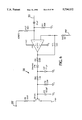
- the bar code scanner 10 includes a scanner 12 for scanning a beam of laser light 13 across a bar code 14.
- the bar code 14 comprising a series of interleaved, or alternating black bars 14b and white spaces 14s, each bar 14b and space 14s having a juxtaposed edge region 14e therebetween.
- the bar code scanner 10 also includes a processor 16 having a light detection section 18 and a multi-bit digitizer 20 for producing a series of edge strength, or timing, pulse signals on output line 17.
- Each one of the timing pulse signals has a time duration, t s , related to reflectivity characteristics of a corresponding one of the edge regions 14e.
- the time duration, t s , of each of the timing pulse signals on line 17 is proportional to the magnitude of the edge strength as measured by the first derivative of the analog signal produced by the light detection section 18 in response to refections of the laser light across through an edge region 14e.
- the multi-bit digitizer 20 also produces a polarity signal on output line 19.
- the polarity signal is a logic signal having a logic state indicative of whether the edge strength pulse produced concurrently therewith is a bar 14b to space 14s edge transitions or, alternatively, a space to bar edge transition.
- a positive edge i.e., the polarity signal changes from a logic 0 to a logic 1
- a negative edge i.e., the polarity signal changes from a logic 1 to a logic 0
- the time duration,t e between leading edges of the timing pulse signals is a measure of the edge to edge time duration of a bar 14b or a space 14s.
- a decoder 21 is provided for decoding the timing pulse and polarity signals on lines 17, 19 into corresponding multi-bit digital words.
- the light detection section 18 includes a detector 22, a differentiator circuit 24, a filter/amplifier stage 26, an automatic gain control (AGC) section 28, and an enhancement filter 30, arranged as shown.
- the detector 22 produces an electrical signal having an amplitude which varies in accordance with the bar code 14 as the beam of light 13 is scanned over the bar code 14. More, particularly, the detector 22 produces an electrical signal 32 (FIG. 3A) having an amplitude which varies in accordance with the reflectivity of the light 13 from the bar code 14 as scanner 12 scans the laser produced beam of light 13 across the bar code 14, the pattern scanned being shown in FIG. 3C.
- the electrical signal 32 amplitude alternates between higher levels 32H 1 , 32H 2 , 32H 3 , 32H 4 , 32H 5 , and 32H 6 and lower levels 32L 1 , 32L 2 , 32L 3 , 32L 4 , and 32L 5 , in response to the beam of light being scanned across the edge regions 14e.
- the differentiator circuit 24 produces an electrical signal 34 on line 25 (FIG. 3B) having an amplitude which varies in accordance with time rates of change in the variations in the amplitude of the detector produced electrical signal 32.
- the differentiator circuit 24 produces a pulse 34 1 -34 10 each time the electrical signal changes between the higher and lower levels 32H 1 -34H 6 , 34L 1 -34L 5 (i.e., 32H 1 -32L 1 , 32L 1 -32H 2 , 32H 2 -32L 2 , 32L 2 -32H 3 . . . , 32L 5 -32H 6 ), respectively, as shown.
- the electrical signal 34 produced by the differentiator circuit 24 is a bipolar signal; that is, negative polarity pulses 34 1 , 34 3 , 34 5 , 34 7 , 34 9 are produced when the electrical signal 32 goes from a high level to a lower level and positive polarity pulses are produced when the electrical signal 32 goes from a lower level to a higher level, as shown. (It is noted that "positive” and negative” are relative to a reference potential, here VREF, as will be described in more detail hereinafter).
- the electrical signal 34 produced by the differentiator circuit 24 is fed, via line 25 to a terminal 25'. Also fed to terminal 25' is the output of AGC circuit 28. The output of terminal 25' is to the filter/amplifier stage 26. The output on filter/amplifier stage 26 is fed, via line 55 to: the input of AGC circuit 28; the input of enhancement filter 30; and, terminal B of switch 75, as shown.
- the enhancement filter 30 modifies the pulses 34 1 -34 10 produced by the differentiator circuit 24; i.e. from signals such as those shown in FIG. 24 to those as shown in FIG. 25. Such modification includes increasing the rise time, and peak level of, the pulses 34 1 -34 10 produced by the differentiator circuit 24.
- the output of the enhancement filter is fed to a second input 57 2 of switch 57.
- the output of switch 57 i.e., line 41, is coupled to either: the output of the enhancement filter 30, as when line 41 is coupled to the input 57 1 of switch 57 (i.e., switch 57 position A); or, on the other hand directly to the output of the filter/amplifier stages 26 as when line 41 is coupled to input 57 2 of switch 57 (i.e., switch position B).
- a signal on line 57 3 from decoder 21 is used to control the A, B switch position of switch 57.
- the enhancement filter 30 When in position A the enhancement filter 30 is used (i.e., "in") and when in position B the enhancement filer 30 is not used (i.e., "out”).
- the decoder 21 places the enhancement filter "in” every N scans, where N is a pre-selected integer, here, for example 3.
- multi-bit digitizer 20 includes a threshold level detector 202 (FIGS. 2 and 15) for rejecting modified pulses 34' 1 -34' 10 having peak levels below a threshold level and for converting only non-rejected modified pulses 34' 1 -34' 10 into the edge strength (i.e., timing) pulse signals and polarity signals on lines 17, 19 respectively.
- each one of the converted edge strength timing pulse signals on line 17 has a time duration related to reflectivity characteristics of a corresponding one of the edge regions 14e (here the peak level of the converted, modified pulses 34').
- the decoder 21 converts the edge strength timing pulse signals on line 17 into a timing signal and using a counter, not shown, to measure the time duration of the edge strength timing pulse signals produced on line 17.
- the multi-bit digitizer 20 includes a margin detection circuit 40, a timing generation circuit 42, and a polarity generation circuit 44, all arranged as shown.
- the margin detector circuit 40 (FIG. 4) is responsive to the signals produced on line 41 and detects the presence of a bar code 14 (FIG. 1).
- the timing generation circuit 42 is responsive to the margin detection circuit 40, and the signals produced on line 41, and produces the series of edge strength timing pulse signals on output line 17.
- the polarity circuit 44 is responsive to the signals produced on line 41, and the margin detection circuit 40, and produces, on line 19, a series of logic signals having logic states related to the whether the edge strength pulse is from a bar to space edge transition or, alternatively, from a space to bar edge transition, respectively, of the scanned bar code 14.
- the width of the edge strength timing pulse signals on line 17 provide the absolute value of the strength of the edges.
- the time from rising edge of one edge strength pulse to the rising edge of the next edge strength pulse is the time, t e , between leading edges of the timing pulse signals and is, as noted above, a measure of the edge to edge time duration of a bar 14b or a space 14s.
- the value (i.e., logic state) of the polarity signal on line 19 at the rising edge of the edge strength timing pulse signals on line 17 represents the polarity of the edge (i.e., whether the edge is a bar 14b or a space 14s, a discussed above.
- the differentiator circuit 24 includes an operational amplifier 45 having the inverting input (-) thereof fed, via line 48, by the detector 22 through a capacitor C27, here 1000 pF, and serially connected resistor R2, here 1k ohm and the non-inverting input (+) fed by a reference potential (VREF), here nominally 1.9 volt s , as shown.
- the reference voltage VREF is derived from a resistor-divider circuit (not shown) and is filtered through a parallel combination of a 2.1 microfarad electrolytic capacitor (not shown) and a 0.1 microfarad ceramic capacitor (not shown)).
- the input line 48 is fed by detector 22 (FIG. 2), i.e., the signal 32 (FIG. 3A).
- a parallel resistor R34-capacitor C23 network 47 is connected between the output and inverting input (-) of the operational amplifier 45, as shown.
- R34 is 100 K ohms and capacitor C23 is 5 pF.
- the gain of the differentiator is here 40 db with poles at 318 kHz and 159 kHz.
- the differentiator circuit 24 has a bandwidth of 40 kHz and produces analog signal levels on line 49 (i.e., signal 34, FIG. 3B) from 10 m V p-p to 1.6 V p-p .
- the filter/amplifier stage 26 is shown in FIG. 5.
- the filter/amplifier stage 26 is a five pole modified Butterworth filter and is used to provide additional signal conditioning to the differentiator circuit 24 output signal on line 49.
- the gain through the stage 26 is 46 db.
- the stage 26 includes three cascaded operational amplifiers 50, 52, 54.
- a first amplifier 50 has the non-inverting (+) input thereof fed by the output of the differentiator circuit 24 via line 49 and the inverting (-) input fed to the 1.9 volt VREF reference potential through a, here 82.5 k ohm resistor R18, as shown.
- a parallel 82.5 k ohm-47 pF resistor R28-capacitor C47 network 56 is provided in a feedback loop, as shown.
- the intermediate amplifier 52 has the inverting input (-) thereof coupled to the output of the first amplifier 50 through an network 58 made up of resistor R106 (here 8.2 k ohms), capacitor C15 (here 0.1 microfarad), grounded capacitor C29 (here 470 pF) and resistor R94, here 20 k ohms, arranged as shown.
- the non-inverting input (+) is coupled to a second reference potential, VFERF, as shown.
- the last amplifier 54 has its inverting input (-) coupled to the output of the intermediate amplifier 52 through a network 68 made up of resistor R50, here 3.9 k ohms, a capacitor C19, here 0.1 microfarad, a grounded capacitor C13, here 2200 pF and a resistor R27, here 18.2 k ohms, arranged as shown.
- the non-inverting input (+) is coupled to the second reference potential, VREF, as shown.
- a feedback network 70 made up of resistors R5, here 39 k ohms, and capacitor C20 here 10 pF, is provided, as shown.
- the AGC circuit 28 is shown in FIG. 6.
- the purpose of the AGC circuit 28 is to provide amplitude regulated analog signals to the multi-bit digitizer 20 (FIG. 2).
- the AGC'd Butterworth filter stage 28 provides a range of gain, here approximately a maximum of 44 db to a minimum of 2.8 dB.
- the AGC'd Butterworth filter stage 26 With signal levels from the output of the differentiator circuit 24 ranging from 10 mV p-p to 1.6 V p-p , the AGC'd Butterworth filter stage 26 provides a maximum signal magnitude for the signal on line 41 of 2.22 V p-p and a minimum signal of 1.66 V p-p , for a maximum to minimum ratio of 1.4.
- the enhancement filter 30 is shown in FIG. 7.
- the purpose for the enhancement filter 30 is to correct for convolution distortion by enhancing, or amplifying, the high frequency content of the analog signal fed thereto while maintaining linear phase. More particularly, the enhancement filter 30 corrects for some of the convolution distortion realized when the spot size of the laser beam 13 (FIG. 1) is significantly larger than the narrowest symbol element (i.e., a bar 14b or a space 14s) in the bar code 14. As the face of the laser beam 13 moves outward from the bar code 14, a typical beam profile in the x-direction (FIG. 1) starts out wide, grows narrow until a minimum is reached at the waist, and then grows larger at farther ranges.
- Convolution distortion is most prominent when high density symbols are placed close to the scanner 12 where the spot size is large, or symbols placed far into the range of scanner 12 where the spot size also becomes large. More particularly, in bar code laser scanning one of the factors limiting the working range of the scanner is the filtering effect of the optical beam on the original bi-level (i.e., bar-space) bar code signal.
- the purpose of an analog edge enhancement filter 30 is to compensate for the effect of the finite width of the optical beam. This effectively gives the scanner higher resolution.
- the optical spot of the laser acts as a low pass filter on the original bar code signal 32 (FIG. 3A) produced by the detector 22. This results in a smoothing of the edges of the signal. If the spot size is larger than the smallest element of the bar code (i.e. a unit module; bar or space) then not only are the edges smoothed but the height of the edges decreases. This can be seen by looking at the signal in FIGS. 8A and 9B, where FIG. 8A is the output signal 32' of detector 22 for a spot size of 2.0 modules and FIG. 9A is the output signals 32" of detector 22 for a spot size of 2.8 modules. Also, as the spot size gets larger, the actual edge locations shift. This is often referred to as convolution distortion.
- the purpose of the enhancement filter 30 is to enhance the edge strengths (i.e., the peaks 34 1 -34 10 , in the signal produced by the differentiator circuit 34 before being passed to the multi-bit digitizer 20 so that the valid edges will exceed the threshold as well as be close enough to the proper location so that the bar code is decodable.
- the peaks in the signals shown in FIGS. 8B and 9B are shown in FIGS. 8C and 9C, respectively.
- the spot size of the laser is a physical length measured in microns or mils. However, since the laser beam is scanning the spot size can be thought of as having a size (or time duration) in seconds.
- the time duration of the spot is the physical size (say in inches) divided by the velocity (say in inches/second). It is convenient to think in the time domain since the received signal is a time domain signal and all subsequent processing (i.e. analog filtering, digitizing, etc.) is done in the time domain.
- the optical spot size changes with distance from the scanner.
- the spot size grow approximately linearly with distance.
- the spot speed of the laser grows linearly as a function of distance from the scanner.
- the spot duration in seconds, is approximately fixed.
- the optical beam is Gaussian
- the impulse response of the low pass filter is Gaussian, ##EQU1## where the spot size in the time domain is 4 ⁇ .
- the Laplace Transform of this impulse response is, ##EQU2##
- Edge enhancement filter 30 is to implemented to an approximate inverse filter of H(s) using a Taylor series approximation: ##EQU3##
- the demoninator, ⁇ (s), gives the pole locations which are usually some standard low pass filter poles (e.g. Butterworth, Bessel). These poles art placed at higher frequencies than the zeros, so to prevent too large a gain at high frequencies that would just increase noise.
- ⁇ (s) usually some standard low pass filter poles (e.g. Butterworth, Bessel).
- FIG. 9 shows the transfer function H(f) due to the optical spot, the transfer function G(f) due to the edge enhancement filter, and the transfer function of the combination H(f)G(f). Note that the bandwidth of the combined system is widened.
- the effect of the edge enhancement filter 30 is to improve the working range of the scanner 12. At distances where the spot size of the laser beam 13 is so large that the strength of the edges are less than the threshold in the multi-bit digitizer 20, or the edges have shifted too much, the bar code is undecodable. As noted above, the edge enhancement filter 30 enhances the edges of the signal so that they will exceed the threshold and be closer to the proper location and the bar code is decodable.
- FIGS. 24 and 25 show signals produced when scanning a high density bar code (e.g. 3.5 mil) several inches from the noise of a standard range scanner.
- FIG. 24 shows the signal produced by the differentiator circuit 24 and FIG. 25 shows the same signal after passing through the enhancement filter 30. It is noted that the edges of the enhanced signal produced by enhancement filter 30 are much more pronounced and it is much easier to digitize and decode such an enhanced signal.
- the enhancement filter 30 includes four modified Butterworth poles, and two complex conjugate pairs of zeros (one pair of complex conjugate zeros to the right of the imaginary axis, the other pair to the left) arranged is such an order to provide linear phase over the ⁇ enhanced ⁇ frequencies of interest.
- such circuit 42 includes: a full wave rectifier circuit (FWR) 200 for converting the bipolar signal on line 41 into a corresponding unipolar electrical signal on line 201.
- the threshold circuit 202 is fed by the unipolar signal on line 201 and by a reference potential produced by the threshold circuit 202 itself to represent a predetermined percentage, here 80% of a peak level in the unipolar signal.
- the threshold circuit 202 produces a logic signal on line 204 related to the difference between the level of the unipolar signal on line 201 and the reference potential.
- the timing generation circuit 42 includes the edge detector circuit 206 (FIG.
- the timing generation circuit 42 includes a timing control logic circuit 210, fed by the edge detector circuit 206, the threshold detector circuit 202 (FIG. 15) and the margin detection circuit 40, for producing the edge strength timing pulse signals on line 17.
- the edge strength pulse commences when a peak in the unipolar signal on line 201 above the threshold level established by the threshold detector 202 is detected and continues for a period of time related to the magnitude of the peak of the unipolar signal, i.e., the peak level of the unipolar signal pulse.
- the polarity generation circuit 44 is responsive to the electrical signal produced by the differentiator circuit 24 (or after modification, if any, by the enhancement filter 30), the electrical signal produced by the margin detection circuit 40, the edge strength timing pulse signal on line 17, and a reference signal on line 212 representative of the average level of the electrical signal produced by the differentiator circuit 24 and, when "in", enhancement filter 30, for producing a logic signal on line 19 having a first logic state signal when the electrical signal produced by the differentiator circuit 22 and, when "in", enhancement filter 30 is greater than the reference signal on line 212 and a second logic state when the electrical signal produced by the differentiator circuit 24 and, when "in", enhancement filter 30 is less than the reference signal on line 212.
- Margin detection circuit 40 detects the presence of a bar code and enables timing and polarity signals to be produced on line 17, 19, respectively.
- Margin detection circuit 40 includes a resistor voltage divider network 214 (R29, R74) fed by a reference voltage VREF, here 1.9 volts. The voltage produced by the network 214 is compared to the enhanced differentiated analog signal produced by the signal on line 41. When the first negative going bar edge (i.e., as the signal 34, FIG. 3A, goes from 32H 1 to 32l 1 ), comparator 216 (FIG. 12) produces a relatively low voltage.
- This low voltage turns “off” transistor Q7, and raises the level of the voltage on the collector electrode thereof (i.e., line 218) to a supply voltage, VREG, through a resistor R119.
- This in turn allows the timing pulse and polarity signals to be produced on lines 17, 19.
- the signal 34 (FIG. 3A) reaches a high steady state level, i.e., 32H 6
- the comparator 216 becomes an open circuit at its output.
- capacitor C6 start charging to VREG through resistor R30.
- the transistor Q7 saturates pulling the collector electrode thereof, and hence line 218, to a "low" level.
- the multi-bit digitizer 20 produces the timing pulse signal on line 17 with the duration proportional to the height of the peaks of the enhanced, differentiated analog signal on line 41. The rising edge of the pulse occurs at the peak of the enhanced, differentiated analog signal on line 41 of the above described threshold conditions are met.
- the FWR 200 includes capacitor C3, resistors R24, R11, R23, R10, R26, a pair of diodes D1, D2, and operational amplifiers 222, 224, all arranged as shown.
- the function of the FWR 200 is as follows: When the enhanced, differentiated analog signal on line 41, (Vin) goes below the reference voltage VREF, diode D1 is forward biased and diode D2 is reversed biased. This sets the voltage at the anode of diode D2 at the reference voltage VREF.
- " is the resistance of the (R26)(R23)/(R26+R23); i.e, the resistance of the parallel combination of resistors R26, R23. Therefore, Vout VREF-Vin.
- D1 is reversed biased and D2 is forward biased. This sets the voltage at the anode of D2 equal to -Vin+VREF.
- .vertline.R23)). Therefore , Vout VREF+Vin. Therefore, the output of the FWR 200 is a unipolar signal relative to the reference voltage, VREF.
- the edge detection circuit 206 As shown. It is first noted that the function of the edge detect circuit 206 is to locate the edges of the enhanced, differentiated analog signal on line 41 which should correlate to the bar/space edges 14s (FIG. 1) of the bar code 14.
- the full waive rectified, enhanced differentiated analog signal on line 201 is fed, through an R-C network 226 made up of a capacitor C1, here 1000 pF and resistor R1, here 1.8 kohms for filtering.
- the RC combination, i.e., network 226, acts as a passive differentiator stage with the result that the peaks (maximums) of the signal on line 201 from FWR 200 get mapped into zeros, i.e. signals having levels at VREF.
- This filtered signal is compared to VREF (1.9 volts) in comparator 228.
- comparator 228 is triggered and produces a high voltage on output 208.
- Resistors R118, R15 and R21 generate hysteresis which prevents the comparator 228 from switching on noise.
- the comparator 228 output 208 switches to a high level every time the differentiated signal produced by network 226 peak is detected.
- the threshold circuit 202 is shown.
- the function of the threshold circuit 202 is to monitor the level of the FWR signal produced on line 201 and switch the output 204 of the threshold circuit 202 to a high level when the level of the signal from FWR 200 (i.e., the level of the signal on line 201) gets above some percentage, here, 80% of the peak voltage level on line 201.
- Comparator 230, diode CR7 and capacitor C42 form a positive peak detector.
- the charge time of capacitor C42 is controlled by the output impedance of comparator 230 in series with the dynamic resistance of diode CR7.
- the discharge time of capacitor C42 is controlled by resistor R83 in series with the parallel combination of resistors R115, R36, as shown.
- the voltage fed to the inverting input (-) of comparator 232 is, therefore, a percentage of the peak voltage on capacitor C42; more particularly, the voltage on the input inverting input (-) of comparator 232 is equal to Vcap(R36/(R36+R83
- the voltage on the input inverting input (-) of comparator 232 is compared to the FWR voltage produced on line 201.
- the voltage on line 201 is fed to the non-inverting (-) input of comparator 232 through resistors R39, as shown.
- the timing generation circuit 42 also includes a timing control and logic circuit 210 (FIG. 16) and an A/D converter circuit 250 (FIG. 17).
- the timing control and logic circuit 210 produces a positive going pulse on line 17 at the peaks produced by the FWR 200 on line 201.
- the timing control logic circuit 210 is shown to include four NAND gates 252, 254, 256 and 258 arranged as shown and configured to be logically equivalent to a single triple input AND gate section 259.
- the inputs to the logic circuit 259 are the outputs of margin detection circuit 40 (i.e, line 218), edge detection circuit 208 (i.e., line 208), and threshold detection circuit 202 (i.e., line 204).
- Lines 204, 208 are fed as inputs to NAND gate 252, the output of which, along with a fixed logic voltage V1, is fed to NAND gate 254, the output of which, along with line 218 is fed to NAND gate 256, as shown.
- the output of logic circuit 259 provides a signal for clock terminal 260 of a D flip-flop 262.
- a clock signal is fed to terminal 260 to clock in a high signal fed to the "D" input terminal of flip/flop 262, thereby producing a high level at the Q output of flip/flop 262, such Q output being fed to line 17.
- the edge strength pulse is commenced on line 17.
- the complementary output Q * goes low.
- the low level signal on the complementary output Q * is fed, via line 270 to the A/D converter 250 (FIGS. 2 and 17).
- the Q * output is fed, via line 270 to pins E3 and E4 of an analog switch 272, here a model HC 4066.
- the A/D converter circuit 250 is enabled when the complementary output Q * goes low. Prior to that event, Q * is high.
- a high level on pins E3 and E4 of analog switch 272 forces the closure of the analog switch and connects input pin A3 to output pin B3 and connects input pin A4 to output pin B4.
- Pin A4 is the output of FWR 200 via line 201.
- Output pin B3 is connected to a resistor-capacitor network 273 made up of capacitor C5, a high input impedance buffer amplifier 275 and resistor R82, as shown.
- capacitor C5 acts as a sampling capacitor, and the signal at input pin A3 (i.e., the output of FWR 200) is fed through the resistor-capacitor network 273 to the non-inverting input of comparator 274, as shown.
- Resistor R32, capacitor C24, and comparator 276 are arranged as shown to form an integrator 277. As long as input pin A4 is connected to output pin B4, the integrator 277 is disabled, and VREF, fed to the non-inverting input (+) of comparator 276, appears at the output of comparator 276 (i.e., on line 278) and therefore at the inverting input (-) of comparator 274.
- comparator 274 When the level of the signal produced at the output of FWR 200 (on line 201) at non-inverting input (+) of comparator 274 is greater than VREF on line 278, the comparator 274 is at a high level. The output of comparator 274 is fed, via line 282, to the clear input of D flip/flop 262 (FIG. 16).
- switch 57 may be implemented with the upper portion of switch 272. More particularly, terminal 57 1 may be connected to terminal A 1 , terminal 57 2 may be connected to terminal A 2 and terminal B 1 (here connected in common with B 2 ) may provide line 41).
- the output terminal Q of the D flip/flop 262 produces the timing pulse signal for decoder 21 (FIG. 1). It gets set by the clocking at the peaks of the signal produced by FWR 200 and reset by the clear signal for the D flip/flop 262 on line 282 from the A/D converter 250 (FIG. 17).
- the time during which the Q terminal of the D flip/flop remains at a high level is proportional to the amplitude of the peaks of the signal produced by FWR 200 on line 201.
- the polarity generation circuit 44 is shown.
- the polarity signal produced by such circuit 44 on line 19 represents the polarity of differentiated analog signal on line 41 at it's peaks.
- the differentiated analog signal on line 41 is compared to VREF (it's ac ground) on line 212 in comparator 290. If the signal on line 41 is above the reference VREF, the output of comparator 290 is at a low level. On the other hand, if the signal on line 41 is below the reference VREF, the output of comparator 290 is at a high level.
- This output acts as data line to a D flip/flop 272.
- Resistors R80, R98, and R60 provide hysteresis and pull up to VREG, as shown.
- the data at the D terminal of the D flip/flop 272 appears as the polarity signal on line 19 at the rising edge of timing pulse signal on line 17. (The signal on line 17 is fed to the clock terminal, CK, of D flip/flop 272, as shown).
- the decoder 21 includes two counters; a 16-bit counter 302 to measure bar code edge-to-edge times, t e (FIG. 1), from the edge strength or timing pulse signal on line 17 and an 8-bit counter 300 to the magnitude of the strength signal (i.e., the time duration t s ) from the signal strength timing pulse signal on line 17.
- the clock rate of the counter 300 is faster than the clock rate for counter 300, here by a factor of 5.
- the decoder 21 reads the two counter values, resets the counters, and stores the values in memory 304 along with the polarity bit of the polarity signal on line 19. The polarity is tested and if it is positive then the strength value is stored directly. If it is negative the decoder stores a negative strength. Once a scan of multi-bit data has been stored it must be decoded. As shown in the timing histories for the example in FIG. 1, the middle two timing pulse P 1 , P 2 signals have the same polarity, as when there are two negative edges in a row.
- the decode algorithm preformed by CPU 306, can be viewed as a pre-process and post-process.
- FIG. 19 shows a flow chart of the decode algorithm.
- the pre-process involves first analyzing the edge strength timing pulse signals to determine edge strength, choosing a noise threshold to separate real and false edges, and then converting the data to a standard DBP format. After a standard decode attempt has been performed on the converted DBP data, the post-process analyzes the decode results and initiates appropriate actions. If a full decode occurred, the post decode analysis will decide whether to accept this decode based on certain security checks. The post-process will also decide whether to attempt a second decode on the same data and whether to place the enhancement filter 30 "in” or "out”.
- the process of converting the Multibit data to DBP is shown in FIG. 20.
- the edge strengths are depicted as vertical lines whose height and direction represent strength and polarity. There are two rules used in the converting process. First, all edges that are below the noise threshold are ignored. Second, if there are multiple edges of the same polarity above the noise threshold, the stronger edge is chosen.
- the single decode attempt processing steps are described below:
- a complete scan of data is acquired through the Timing, Polarity, and start of scan (SOS) signals (FIG. 1) and loaded into memory 304.
- the data consists of a sequence of edges (positive or negative) and edge strengths;
- histograms are constructed using the magnitude of the edge strengths.
- the histograms' peaks and valleys are analyzed and stored as histogram features. Valleys in the histograms represent possible conversion thresholds. Edges whose strengths are below the conversion threshold are considered noise and are ignored; and,
- the time between edges, t e are measured using 16 bit timers.
- the 16 bit data is scaled down to 8 bits. The amount of scaling is chosen based on the center ten elements of the DBP data;
- the Multibit data After the Multibit data has been converted into a standard DBP format, it is processed by the standard 8-bit decode algorithms.
- the standard decode algorithms are slightly modified in order to return detailed information about a failed decode attempt (eg. how many characters were decoded ?). This information is used by the post decode analysis;
- the post decode analysis examines the decode results, the noise measure, and the histogram features and initiates appropriate actions. If a full decode occurred, the post process will decide whether to accept this decode based on the decoded message and the noise measure (number of edges ignored). For example, "weak" code types such as Interleaved 2 of 5 may be rejected if a large amount noise is present. The post decode analysis will also decide whether to attempt a second decode on the same Multibit data and whether the enhancement filter should be turned "on” (i.e., "in”) or "off” (i.e. "out”).
- edges are ⁇ real ⁇ as opposed to those which were caused by noise.
- histograms (FIG. 21) of the edge strengths are used. Typically, these histograms have two main peaks; one peak consisting of the weaker edges represents the noise, the other, consisting of the stronger edges, represent barcode. The lowest point in the valley between the two peaks is the noise threshold (edges stronger than the threshold are considered real).
- the edge strength histogram consists of a 128 byte array. Each element of this array represents a possible edge strength (0-127). The value of each element in the array represent the number of occurrences of edges having that strength. To create the histogram, the MultiBit load is traversed and, using each strength as an index into the array, the appropriate histogram location is incremented;
- the initial histogram (FIG. 21) tends to be very coarse in distribution, having many high peaks and deep valleys. This make it difficult for the software to determine which of these are the true peaks and valleys.
- the histogram is smoothed (FIG. 22) using a rolling sum technique.
- each location represents the sum of four consecutive locations of the original histogram.
- Each consecutive sum in the smoothed histogram overlaps the previous sum by three locations of the original histogram. For example:
- each peak and valley is identified.
- a peak is defined as any location whose immediate neighbors are smaller.
- a valley is defined as any location whose immediate neighbors are larger. In cases where an immediate neighbor is equal, the nearest non-equal neighbor is used for the determination. When a peak or valley has a neighbor which is equal, the left-most location is selected;
- peak and valley thresholds are chosen. Only valleys that are below the valley threshold are considered. Likewise, only peaks which are above the peak threshold are considered.
- the peak threshold is determined by taking the average of all the peaks heights greater than 4, excluding the highest peak and the lowest peak (which is greater than 4). This vale is then biased by negative 2 to accept borderline peaks. If there are less than 5 peaks which are greater than 4, the threshold is set to the lowest peak which is greater than 4. If only there is only 1 peak greater than 4, the threshold is set to that value minus 1. Only those peaks which are greater than the threshold are considered in the following steps.
- the valley threshold is determined by taking the average of all the valley depths greater than 0, excluding the highest valley and the lowest valley (which is greater than 0). This value is then biased by positive 2 to accept borderline valleys. If there are less than 5 valleys which are greater than 0, the threshold is set to the highest valley which is greater than 0. If only there is only 1 valley greater than 0, the threshold is set to that value plus 1. Only those valleys which are less than the threshold are considered in the following steps. In cases where the peak threshold is less than the valley threshold, the following rule applies. If there were more peaks found than valleys, set the valley threshold qual to the peak threshold. Otherwise, if there were more valleys than peaks, then set the peak threshold equal to the valley threshold.
- the four locations in the original unsmoothed histogram which represent the selected point are examined. The lowest of the four locations is selected as the threshold. If more than one of those location shares the lowest value, the left-most location is selected. This value is then decremented so that strengths equal to the lowest point are accepted as real data during the conversion process.
- the data can be converted to standard DBP format for decoding by the standard decode algorithms described in the above referenced patent applications, the subject matter of which is incorporated herein by reference). This is done by traversing the load and concantinating edges that do not exceed the noise threshold which fall between edges, of alternating polarity, that do.
- timing pulse signals 400, 402, 404, 406, 408, and 410 are shown having edge strength levels, 20, 18, 9, 11, 22, and 21, respectively, as indicated.
- the corresponding polarity signal is indicated in FIG. 26B.
- the decoder ignores timing pulse 404, as indicted in FIG. 26C.
- timing pulse signal 420, 422, 424, 426, 428, 430 and 432 are shown having edge strength levels 20, 16, 68, 18, 17, 23 and 19, respectively, as indicated, in FIG. 27A.
- a threshold level is 15, for example.
- timing pulse signal 424 does not exceed the threshold level of 15, and is ignored, as described above.
- two consecutive timing pulse signals, 428, 430 have the same edge polarity, as shown in FIG. 27B.
- timing pulse signal having the strongest edge strength level here timing pulse 430 is selected as the timing pulse to determine polarity (i.e., the converted DBP signal FIG. 27C) changes state in response to the stronger edges strength; i.e., timing pulse signal 430, as shown in FIG. 26C
- the edge enhancement filter 30 (FIG. 3) can be switched “in” or “out” under software control. When switched “in”, this filter 30 increases the scanners ability to read high density symbols, as discussed above. However, with the filter 30 "in”, the scanners ability to read poorly printed dot matrix symbols is reduced. Preferably, the edge enhancement filter 30 is switched “in” every third scan for the duration of one scan. This is done to ensure that the filter is active on alternating scan directions. In cases where multiple decodes are required, once a decode has occurred the filter will be left in the state it has in at the time of the initial decode.
Abstract
Description
vout=(1/C24)(∫ARCREF2/R32)dt+ARCREF2)
smoothed.sub.-- hist 0!=hist 0!+hist 1!+hist 2!+hist 3!
smoothed.sub.-- hist 0!=hist 1!+hist 2!+hist 3!+hist 4!;
Claims (18)
Priority Applications (8)
| Application Number | Priority Date | Filing Date | Title |
|---|---|---|---|
| US08/454,830 US5734152A (en) | 1995-05-31 | 1995-05-31 | Optical scanners and signal processors therefor |
| EP19960303984 EP0745951B1 (en) | 1995-05-31 | 1996-05-31 | Optical scanners |
| DE1996637397 DE69637397T2 (en) | 1995-05-31 | 1996-05-31 | Optical barcode scanner |
| DE1996636205 DE69636205T2 (en) | 1995-05-31 | 1996-05-31 | Optical scanner |
| EP04075636A EP1445725B1 (en) | 1995-05-31 | 1996-05-31 | Optical scanner |
| EP04075635A EP1443450B1 (en) | 1995-05-31 | 1996-05-31 | Optical barcode scanner |
| DE1996634584 DE69634584T2 (en) | 1995-05-31 | 1996-05-31 | Optical scanner |
| US09/436,468 US6209788B1 (en) | 1992-04-02 | 1999-11-08 | Optical scanners |
Applications Claiming Priority (1)
| Application Number | Priority Date | Filing Date | Title |
|---|---|---|---|
| US08/454,830 US5734152A (en) | 1995-05-31 | 1995-05-31 | Optical scanners and signal processors therefor |
Related Parent Applications (2)
| Application Number | Title | Priority Date | Filing Date |
|---|---|---|---|
| US08/436,468 Continuation US5603095A (en) | 1993-09-27 | 1994-09-27 | Radio system and a subscriber terminal for a radio system |
| US08/455,216 Continuation US6170749B1 (en) | 1992-04-02 | 1995-05-31 | Method of scanning indicia using selective sampling |
Related Child Applications (1)
| Application Number | Title | Priority Date | Filing Date |
|---|---|---|---|
| US08/335,001 Continuation US6082621A (en) | 1992-04-02 | 1994-11-09 | Interface between threshold processing digitizer for bar code reader |
Publications (1)
| Publication Number | Publication Date |
|---|---|
| US5734152A true US5734152A (en) | 1998-03-31 |
Family
ID=23806284
Family Applications (1)
| Application Number | Title | Priority Date | Filing Date |
|---|---|---|---|
| US08/454,830 Expired - Lifetime US5734152A (en) | 1992-04-02 | 1995-05-31 | Optical scanners and signal processors therefor |
Country Status (1)
| Country | Link |
|---|---|
| US (1) | US5734152A (en) |
Cited By (23)
| Publication number | Priority date | Publication date | Assignee | Title |
|---|---|---|---|---|
| US5914478A (en) * | 1997-01-24 | 1999-06-22 | Symbol Technologies, Inc. | Scanning system and method of operation with intelligent automatic gain control |
| US6324303B1 (en) * | 1996-08-07 | 2001-11-27 | Central Research Laboratories Limited | Method and apparatus for coding information |
| US6328213B1 (en) | 1998-06-12 | 2001-12-11 | Symbol Technologies, Inc. | Method of processing an analog electrical signal containing information representative of reflected light from coded indicia, wherein the electrical signal contains edge transitions |
| US6371373B1 (en) * | 1999-05-25 | 2002-04-16 | Matsushita Electric Industrial Co., Ltd. | Method for reading a two-dimensional barcode |
| US20020056753A1 (en) * | 2000-11-14 | 2002-05-16 | Michele Benedetti | Method for locating the transitions between the elements of a bar code |
| US6540145B2 (en) | 1999-06-11 | 2003-04-01 | Symbol Technologies, Inc. | Aperture controlled laser beam shaping techniques for scanning optical code |
| US6616040B1 (en) * | 1995-12-18 | 2003-09-09 | Metrologic Instruments, Inc. | Analog scan data signal processor employing a time-domain substrate noise filter for non-linearly processing analog scan data signals and reducing substrate noise signal levels therein prior to first derivative signal generation and processing operations carried out within said analog scan data signal processor |
| US6616046B1 (en) | 2000-05-10 | 2003-09-09 | Symbol Technologies, Inc. | Techniques for miniaturizing bar code scanners including spiral springs and speckle noise reduction |
| US6633433B2 (en) | 1999-06-11 | 2003-10-14 | Symbol Technologies, Inc. | Beam shaping for optical scanners |
| US6651888B1 (en) | 1999-02-02 | 2003-11-25 | Symbol Technologies, Inc. | Beam shaping system and diverging laser beam for scanning optical code |
| US20050006479A1 (en) * | 1998-06-12 | 2005-01-13 | Symbol Technologies, Inc. | Digitizing bar code symbol data |
| US20050018060A1 (en) * | 2003-07-23 | 2005-01-27 | Isao Takayanagi | On-chip image processing |
| US20050236485A1 (en) * | 2004-04-26 | 2005-10-27 | Dayou Wang | Gain control system and method for use in electro-optical readers |
| US20050274808A1 (en) * | 2004-06-10 | 2005-12-15 | Olmstead Bryan L | System, circuit, and method for edge detection in a binary optical code |
| US20050274809A1 (en) * | 2004-06-10 | 2005-12-15 | Colley James E | System, circuit, and method for edge detection in a binary optical code |
| US20060043192A1 (en) * | 2004-08-31 | 2006-03-02 | Symbol Technologies, Inc. | Transmitting enhanced scanner signals on a single channel |
| US7093763B1 (en) * | 2005-02-25 | 2006-08-22 | Symbol Technologies, Inc. | Laser scanner having analog digitizer with increased noise immunity |
| US20060218766A1 (en) * | 2005-03-30 | 2006-10-05 | Marlow Leonard G Jr | Ductmate clip setter |
| US20060239555A1 (en) * | 2005-04-25 | 2006-10-26 | Destiny Technology Corporation | System and method for differentiating pictures and texts |
| WO2006127195A1 (en) * | 2005-05-26 | 2006-11-30 | Symbol Technologies, Inc. | Method and system for decoding a barcode |
| US20070158426A1 (en) * | 2004-04-16 | 2007-07-12 | Kolstad Jesse J | Barcode scanner with linear automatic gain control (AGC), modulation transfer function detector, and selectable noise filter |
| US8950678B2 (en) | 2010-11-17 | 2015-02-10 | Hand Held Products, Inc. | Barcode reader with edge detection enhancement |
| US10615732B2 (en) * | 2017-12-27 | 2020-04-07 | Commissariat A L'energie Atomique Et Aux Energies Alternatives | Method for pulse width modulation |
Citations (37)
| Publication number | Priority date | Publication date | Assignee | Title |
|---|---|---|---|---|
| US3796862A (en) * | 1971-09-27 | 1974-03-12 | Ncr | Bar code reader |
| US3798458A (en) * | 1972-10-30 | 1974-03-19 | Ibm | Optical scanner including an aperture design for non-synchronous detection of bar codes |
| US3892949A (en) * | 1974-04-22 | 1975-07-01 | Rca Corp | Circuit for determining the time of transitions in an alternating signal |
| US3932840A (en) * | 1973-10-15 | 1976-01-13 | Taplin Business Machines Incorporated | Error detection and sequence maintaining system for bar-code readers |
| US4160156A (en) * | 1978-05-04 | 1979-07-03 | Msi Data Corporation | Method and apparatus for reading bar coded data wherein the light source is periodically energized |
| US4184179A (en) * | 1978-02-24 | 1980-01-15 | Cubic Western Data | Reproduction of binary signals from a recording medium that may be read at varying speeds |
| US4251798A (en) * | 1978-05-31 | 1981-02-17 | Symbol Technologies | Portable laser scanning arrangement for and method of evaluating and validating bar code symbols |
| EP0036950A1 (en) * | 1980-03-06 | 1981-10-07 | R.J. Reynolds Tobacco Company | Dynamic threshold detector |
| US4354101A (en) * | 1977-04-15 | 1982-10-12 | Msi Data Corporation | Method and apparatus for reading and decoding a high density linear bar code |
| US4360798A (en) * | 1978-05-31 | 1982-11-23 | Symbol Technologies, Inc. | Portable laser scanning arrangement for and method of evaluating and validating bar code symbols |
| US4369361A (en) * | 1980-03-25 | 1983-01-18 | Symbol Technologies, Inc. | Portable, stand-alone, desk-top laser scanning workstation for intelligent data acquisition terminal and method of scanning |
| US4387297A (en) * | 1980-02-29 | 1983-06-07 | Symbol Technologies, Inc. | Portable laser scanning system and scanning methods |
| US4409470A (en) * | 1982-01-25 | 1983-10-11 | Symbol Technologies, Inc. | Narrow-bodied, single-and twin-windowed portable laser scanning head for reading bar code symbols |
| US4460120A (en) * | 1982-01-25 | 1984-07-17 | Symbol Technologies, Inc. | Narrow bodied, single- and twin-windowed portable laser scanning head for reading bar code symbols |
| US4496831A (en) * | 1980-02-29 | 1985-01-29 | Symbol Technologies, Inc. | Portable laser scanning system and scanning methods |
| US4500776A (en) * | 1982-11-08 | 1985-02-19 | Vadim Laser | Method and apparatus for remotely reading and decoding bar codes |
| US4740675A (en) * | 1986-04-10 | 1988-04-26 | Hewlett-Packard Company | Digital bar code slot reader with threshold comparison of the differentiated bar code signal |
| US4746789A (en) * | 1984-11-02 | 1988-05-24 | U.S. Philips Corporation | Reading device for bar codes |
| US4758717A (en) * | 1982-01-25 | 1988-07-19 | Symbol Technologies, Inc. | Narrow-bodied, single-and twin-windowed portable laser scanning head for reading bar code symbols |
| US4760248A (en) * | 1985-02-28 | 1988-07-26 | Symbol Technologies, Inc. | Portable laser diode scanning head |
| US4782220A (en) * | 1986-09-29 | 1988-11-01 | Mars, Incorporated | Method and apparatus for bar code data autodiscrimination |
| US4798943A (en) * | 1986-09-30 | 1989-01-17 | Spectra-Physics, Inc. | Method and system for control of a bar code scanner threshold |
| US4808804A (en) * | 1987-01-28 | 1989-02-28 | Symbol Technologies, Inc. | Bar code symbol readers with variable spot size and/or working distance |
| US4855581A (en) * | 1988-06-17 | 1989-08-08 | Microscan Systems Incorporated | Decoding of barcodes by preprocessing scan data |
| US4859840A (en) * | 1987-10-30 | 1989-08-22 | Alps Electric Co., Ltd. | Code reading apparatus |
| US4896026A (en) * | 1988-10-31 | 1990-01-23 | Symbol Technologies, Inc. | Laser diode scanner with improved shock mounting |
| US4933538A (en) * | 1988-10-21 | 1990-06-12 | Symbol Technologies, Inc. | Scanning system with adjustable light output and/or scanning angle |
| US4973829A (en) * | 1988-11-22 | 1990-11-27 | Eastman Kodak Company | Bar code reading method |
| US5010242A (en) * | 1989-05-08 | 1991-04-23 | Mars Incorporated | Method and apparatus for variable speed scanning of bar codes |
| US5029183A (en) * | 1989-06-29 | 1991-07-02 | Symbol Technologies, Inc. | Packet data communication network |
| US5036183A (en) * | 1988-08-25 | 1991-07-30 | Alps Electric Co., Ltd. | Code reading device |
| US5059773A (en) * | 1988-11-16 | 1991-10-22 | The Japan Steel Works, Ltd. | Bar code reader signal processing method and device |
| US5073954A (en) * | 1989-02-28 | 1991-12-17 | Electrocom Automation, Inc. | Bar code location and recognition processing system |
| US5128527A (en) * | 1989-03-29 | 1992-07-07 | Fujitsu Limited | Apparatus for reading a bar code |
| US5140146A (en) * | 1989-11-20 | 1992-08-18 | Symbol Technologies, Inc. | Bar code symbol reader with modulation enhancement |
| US5302813A (en) * | 1992-04-02 | 1994-04-12 | Symbol Technologies, Inc. | Multi-bit digitizer |
| US5457309A (en) * | 1994-03-18 | 1995-10-10 | Hand Held Products | Predictive bar code decoding system and method |
-
1995
- 1995-05-31 US US08/454,830 patent/US5734152A/en not_active Expired - Lifetime
Patent Citations (38)
| Publication number | Priority date | Publication date | Assignee | Title |
|---|---|---|---|---|
| US3796862A (en) * | 1971-09-27 | 1974-03-12 | Ncr | Bar code reader |
| US3798458A (en) * | 1972-10-30 | 1974-03-19 | Ibm | Optical scanner including an aperture design for non-synchronous detection of bar codes |
| US3932840A (en) * | 1973-10-15 | 1976-01-13 | Taplin Business Machines Incorporated | Error detection and sequence maintaining system for bar-code readers |
| US3892949A (en) * | 1974-04-22 | 1975-07-01 | Rca Corp | Circuit for determining the time of transitions in an alternating signal |
| US4354101A (en) * | 1977-04-15 | 1982-10-12 | Msi Data Corporation | Method and apparatus for reading and decoding a high density linear bar code |
| US4184179A (en) * | 1978-02-24 | 1980-01-15 | Cubic Western Data | Reproduction of binary signals from a recording medium that may be read at varying speeds |
| US4160156A (en) * | 1978-05-04 | 1979-07-03 | Msi Data Corporation | Method and apparatus for reading bar coded data wherein the light source is periodically energized |
| US4251798A (en) * | 1978-05-31 | 1981-02-17 | Symbol Technologies | Portable laser scanning arrangement for and method of evaluating and validating bar code symbols |
| US4360798A (en) * | 1978-05-31 | 1982-11-23 | Symbol Technologies, Inc. | Portable laser scanning arrangement for and method of evaluating and validating bar code symbols |
| US4387297A (en) * | 1980-02-29 | 1983-06-07 | Symbol Technologies, Inc. | Portable laser scanning system and scanning methods |
| US4387297B1 (en) * | 1980-02-29 | 1995-09-12 | Symbol Technologies Inc | Portable laser scanning system and scanning methods |
| US4496831A (en) * | 1980-02-29 | 1985-01-29 | Symbol Technologies, Inc. | Portable laser scanning system and scanning methods |
| EP0036950A1 (en) * | 1980-03-06 | 1981-10-07 | R.J. Reynolds Tobacco Company | Dynamic threshold detector |
| US4369361A (en) * | 1980-03-25 | 1983-01-18 | Symbol Technologies, Inc. | Portable, stand-alone, desk-top laser scanning workstation for intelligent data acquisition terminal and method of scanning |
| US4758717A (en) * | 1982-01-25 | 1988-07-19 | Symbol Technologies, Inc. | Narrow-bodied, single-and twin-windowed portable laser scanning head for reading bar code symbols |
| US4460120A (en) * | 1982-01-25 | 1984-07-17 | Symbol Technologies, Inc. | Narrow bodied, single- and twin-windowed portable laser scanning head for reading bar code symbols |
| US4409470A (en) * | 1982-01-25 | 1983-10-11 | Symbol Technologies, Inc. | Narrow-bodied, single-and twin-windowed portable laser scanning head for reading bar code symbols |
| US4500776A (en) * | 1982-11-08 | 1985-02-19 | Vadim Laser | Method and apparatus for remotely reading and decoding bar codes |
| US4746789A (en) * | 1984-11-02 | 1988-05-24 | U.S. Philips Corporation | Reading device for bar codes |
| US4760248A (en) * | 1985-02-28 | 1988-07-26 | Symbol Technologies, Inc. | Portable laser diode scanning head |
| US4740675A (en) * | 1986-04-10 | 1988-04-26 | Hewlett-Packard Company | Digital bar code slot reader with threshold comparison of the differentiated bar code signal |
| US4782220A (en) * | 1986-09-29 | 1988-11-01 | Mars, Incorporated | Method and apparatus for bar code data autodiscrimination |
| US4798943A (en) * | 1986-09-30 | 1989-01-17 | Spectra-Physics, Inc. | Method and system for control of a bar code scanner threshold |
| US4808804A (en) * | 1987-01-28 | 1989-02-28 | Symbol Technologies, Inc. | Bar code symbol readers with variable spot size and/or working distance |
| US4859840A (en) * | 1987-10-30 | 1989-08-22 | Alps Electric Co., Ltd. | Code reading apparatus |
| US4855581A (en) * | 1988-06-17 | 1989-08-08 | Microscan Systems Incorporated | Decoding of barcodes by preprocessing scan data |
| US5036183A (en) * | 1988-08-25 | 1991-07-30 | Alps Electric Co., Ltd. | Code reading device |
| US4933538A (en) * | 1988-10-21 | 1990-06-12 | Symbol Technologies, Inc. | Scanning system with adjustable light output and/or scanning angle |
| US4896026A (en) * | 1988-10-31 | 1990-01-23 | Symbol Technologies, Inc. | Laser diode scanner with improved shock mounting |
| US5059773A (en) * | 1988-11-16 | 1991-10-22 | The Japan Steel Works, Ltd. | Bar code reader signal processing method and device |
| US4973829A (en) * | 1988-11-22 | 1990-11-27 | Eastman Kodak Company | Bar code reading method |
| US5073954A (en) * | 1989-02-28 | 1991-12-17 | Electrocom Automation, Inc. | Bar code location and recognition processing system |
| US5128527A (en) * | 1989-03-29 | 1992-07-07 | Fujitsu Limited | Apparatus for reading a bar code |
| US5010242A (en) * | 1989-05-08 | 1991-04-23 | Mars Incorporated | Method and apparatus for variable speed scanning of bar codes |
| US5029183A (en) * | 1989-06-29 | 1991-07-02 | Symbol Technologies, Inc. | Packet data communication network |
| US5140146A (en) * | 1989-11-20 | 1992-08-18 | Symbol Technologies, Inc. | Bar code symbol reader with modulation enhancement |
| US5302813A (en) * | 1992-04-02 | 1994-04-12 | Symbol Technologies, Inc. | Multi-bit digitizer |
| US5457309A (en) * | 1994-03-18 | 1995-10-10 | Hand Held Products | Predictive bar code decoding system and method |
Non-Patent Citations (12)
| Title |
|---|
| Ehrich et al., "Representation of Random Waveforms by Relational Trees," IEEE Transactions on Computers, vol. C-25, No. 7, pp. 725-736 (Jul. 1976). |
| Ehrich et al., Representation of Random Waveforms by Relational Trees, IEEE Transactions on Computers, vol. C 25, No. 7, pp. 725 736 (Jul. 1976). * |
| Eklundh et al., "Peak Detection Using Difference Operators," IEEE Transactions on Pattern Analysis and Machine Intelligence, vol. PAMI-1, No. 3, PP. 317-325 (Jul. 1979). |
| Eklundh et al., Peak Detection Using Difference Operators, IEEE Transactions on Pattern Analysis and Machine Intelligence, vol. PAMI 1, No. 3, PP. 317 325 (Jul. 1979). * |
| Horowitz, "A Syntactic Algorithm for Peak Detection in Waveforms with Applications to Cardiography," Communications of the ACM, vol. 18, No. 5 (May 1975). |
| Horowitz, A Syntactic Algorithm for Peak Detection in Waveforms with Applications to Cardiography, Communications of the ACM, vol. 18, No. 5 (May 1975). * |
| Kiryati et al., "Gray Levels Can Improve the Performance of Binary Image Digitizer," CVGIP: Graphical Models and Image Processing, vol. 53, No. 1, pp. 31-39 (Jan. 1991). |
| Kiryati et al., Gray Levels Can Improve the Performance of Binary Image Digitizer, CVGIP: Graphical Models and Image Processing, vol. 53, No. 1, pp. 31 39 (Jan. 1991). * |
| Pavlidis et al., "Fundamentals of Bar Code Information Theory," Computer, pp. 74-86 (Apr. 1990). |
| Pavlidis et al., Fundamentals of Bar Code Information Theory, Computer, pp. 74 86 (Apr. 1990). * |
| Pavlidis, "Algorithms for Shape Analysis of Contours and Waveforms," IEEE Transactions on Pattern Analysis and Machine Intelligence, vol. PAMI-2, No. 4, pp. 301-312 (Jul. 1980). |
| Pavlidis, Algorithms for Shape Analysis of Contours and Waveforms, IEEE Transactions on Pattern Analysis and Machine Intelligence, vol. PAMI 2, No. 4, pp. 301 312 (Jul. 1980). * |
Cited By (37)
| Publication number | Priority date | Publication date | Assignee | Title |
|---|---|---|---|---|
| US6616040B1 (en) * | 1995-12-18 | 2003-09-09 | Metrologic Instruments, Inc. | Analog scan data signal processor employing a time-domain substrate noise filter for non-linearly processing analog scan data signals and reducing substrate noise signal levels therein prior to first derivative signal generation and processing operations carried out within said analog scan data signal processor |
| US6324303B1 (en) * | 1996-08-07 | 2001-11-27 | Central Research Laboratories Limited | Method and apparatus for coding information |
| US5914478A (en) * | 1997-01-24 | 1999-06-22 | Symbol Technologies, Inc. | Scanning system and method of operation with intelligent automatic gain control |
| US6328213B1 (en) | 1998-06-12 | 2001-12-11 | Symbol Technologies, Inc. | Method of processing an analog electrical signal containing information representative of reflected light from coded indicia, wherein the electrical signal contains edge transitions |
| US20050006479A1 (en) * | 1998-06-12 | 2005-01-13 | Symbol Technologies, Inc. | Digitizing bar code symbol data |
| US7147161B2 (en) | 1998-06-12 | 2006-12-12 | Symbol Technologies, Inc. | Digitizing bar code symbol data |
| US6651888B1 (en) | 1999-02-02 | 2003-11-25 | Symbol Technologies, Inc. | Beam shaping system and diverging laser beam for scanning optical code |
| US6371373B1 (en) * | 1999-05-25 | 2002-04-16 | Matsushita Electric Industrial Co., Ltd. | Method for reading a two-dimensional barcode |
| US6633433B2 (en) | 1999-06-11 | 2003-10-14 | Symbol Technologies, Inc. | Beam shaping for optical scanners |
| US6540145B2 (en) | 1999-06-11 | 2003-04-01 | Symbol Technologies, Inc. | Aperture controlled laser beam shaping techniques for scanning optical code |
| US6616046B1 (en) | 2000-05-10 | 2003-09-09 | Symbol Technologies, Inc. | Techniques for miniaturizing bar code scanners including spiral springs and speckle noise reduction |
| US6834806B2 (en) * | 2000-11-14 | 2004-12-28 | Datalogic S.P.A. | Method for locating the transitions between the elements of a bar code |
| US20020056753A1 (en) * | 2000-11-14 | 2002-05-16 | Michele Benedetti | Method for locating the transitions between the elements of a bar code |
| US20050018060A1 (en) * | 2003-07-23 | 2005-01-27 | Isao Takayanagi | On-chip image processing |
| US20070158426A1 (en) * | 2004-04-16 | 2007-07-12 | Kolstad Jesse J | Barcode scanner with linear automatic gain control (AGC), modulation transfer function detector, and selectable noise filter |
| US7832644B2 (en) * | 2004-04-16 | 2010-11-16 | Microscan Systems, Inc. | Barcode scanner with linear automatic gain control (AGC), modulation transfer function detector, and selectable noise filter |
| US7743993B2 (en) | 2004-04-16 | 2010-06-29 | Microscan Systems, Inc. | Barcode scanner with linear automatic gain control (AGC), modulation transfer function detector, and selectable noise filter |
| US20070215707A1 (en) * | 2004-04-16 | 2007-09-20 | Kolstad Jesse J | Barcode scanner with linear automatic gain control (AGC), modulation transfer function detector, and selectable noise filter |
| US7172125B2 (en) * | 2004-04-26 | 2007-02-06 | Symbol Technologies, Inc. | Gain control system and method for use in electro-optical readers |
| US20050236485A1 (en) * | 2004-04-26 | 2005-10-27 | Dayou Wang | Gain control system and method for use in electro-optical readers |
| US20050274809A1 (en) * | 2004-06-10 | 2005-12-15 | Colley James E | System, circuit, and method for edge detection in a binary optical code |
| US7204422B2 (en) | 2004-06-10 | 2007-04-17 | Psc Scanning, Inc. | System, circuit, and method for edge detection in a binary optical code |
| US7201322B2 (en) | 2004-06-10 | 2007-04-10 | Psc Scanning, Inc. | System, circuit, and method for edge detection in a binary optical code |
| US20050274808A1 (en) * | 2004-06-10 | 2005-12-15 | Olmstead Bryan L | System, circuit, and method for edge detection in a binary optical code |
| US20080121714A1 (en) * | 2004-08-31 | 2008-05-29 | Symbol Technologies, Inc. | Transmitting Enhanced Scanner Signals on a Single Channel |
| US7299985B2 (en) * | 2004-08-31 | 2007-11-27 | Symbol Technologies, Inc. | Transmitting enhanced scanner signals on a single channel |
| US20060043192A1 (en) * | 2004-08-31 | 2006-03-02 | Symbol Technologies, Inc. | Transmitting enhanced scanner signals on a single channel |
| US20060192012A1 (en) * | 2005-02-25 | 2006-08-31 | Symbol Technologies, Inc. | Laser scanner having analog digitizer with increased noise immunity |
| US7093763B1 (en) * | 2005-02-25 | 2006-08-22 | Symbol Technologies, Inc. | Laser scanner having analog digitizer with increased noise immunity |
| US20060218766A1 (en) * | 2005-03-30 | 2006-10-05 | Marlow Leonard G Jr | Ductmate clip setter |
| US20060239555A1 (en) * | 2005-04-25 | 2006-10-26 | Destiny Technology Corporation | System and method for differentiating pictures and texts |
| US20060266837A1 (en) * | 2005-05-26 | 2006-11-30 | Dariusz Madej | Method and system for decoding a barcode |
| WO2006127195A1 (en) * | 2005-05-26 | 2006-11-30 | Symbol Technologies, Inc. | Method and system for decoding a barcode |
| CN101208706B (en) * | 2005-05-26 | 2011-06-08 | 讯宝科技公司 | Method and system for decoding a barcode |
| US8047440B2 (en) * | 2005-05-26 | 2011-11-01 | Symbol Technologies, Inc. | Method and system for decoding a barcode |
| US8950678B2 (en) | 2010-11-17 | 2015-02-10 | Hand Held Products, Inc. | Barcode reader with edge detection enhancement |
| US10615732B2 (en) * | 2017-12-27 | 2020-04-07 | Commissariat A L'energie Atomique Et Aux Energies Alternatives | Method for pulse width modulation |
Similar Documents
| Publication | Publication Date | Title |
|---|---|---|
| US5734152A (en) | Optical scanners and signal processors therefor | |
| US6164540A (en) | Optical scanners | |
| Joseph et al. | Bar code waveform recognition using peak locations | |
| EP1443450B1 (en) | Optical barcode scanner | |
| US4542528A (en) | OCR and bar code reader with optimized sensor | |
| US4402088A (en) | OCR And bar code reading using area array | |
| US4408344A (en) | OCR and Bar code reader using multi port matrix array | |
| EP0531577B1 (en) | Analog waveform decoder | |
| US6547142B1 (en) | Method of scanning indicia using selective sampling | |
| Shellhammer et al. | Novel signal-processing techniques in barcode scanning | |
| EP1114391B1 (en) | Fast edge detection system tolerant of high degree of intersymbol interference | |
| EP0821317A2 (en) | Method and system for decoding distorted image and symbology data | |
| US6012640A (en) | Rule based and fuzzy logic method and apparatus for processing reflectance signals from machine-readable symbols or images | |
| EP0253264B1 (en) | Binary coding circuit for ocr | |
| EP0063243B1 (en) | Ocr and bar code reader with optimized sensor | |
| US5637853A (en) | Reading indicia by analysis of different light reflecting portions based on signal-to-noise ratios | |
| US6164542A (en) | Method and apparatus for decoding unresolved symbol profiles produced from a reduced data set | |
| JPS63165979A (en) | Binarizing circuit for bar code signal | |
| Cai | A new decode algorithm for binary bar codes | |
| EP1205874B1 (en) | Methods and apparatus for area weighted mean processing of barcode signals | |
| JP3095437B2 (en) | Character line detection cutout device and character reading device | |
| EP0268983B1 (en) | Binary coding circuit | |
| Madej | Reversing convolution distortion in a laser bar code scanner | |
| JPH065548B2 (en) | Bar Code Reader Signal Processing Method | |
| US5835984A (en) | Optical scanner employing smart pixel array |
Legal Events
| Date | Code | Title | Description |
|---|---|---|---|
| AS | Assignment |
Owner name: SYMBOL TECHNOLOGIES, INC., NEW YORK Free format text: ASSIGNMENT OF ASSIGNORS INTEREST;ASSIGNORS:GOREN, DAVID;SHELLHAMMER, STEPHEN;KUCHENBROD, HARRY;AND OTHERS;REEL/FRAME:007599/0715;SIGNING DATES FROM 19950714 TO 19950724 |
|
| STCF | Information on status: patent grant |
Free format text: PATENTED CASE |
|
| CC | Certificate of correction | ||
| FPAY | Fee payment |
Year of fee payment: 4 |
|
| AS | Assignment |
Owner name: JPMORGAN CHASE BANK, N.A., NEW YORK Free format text: SECURITY INTEREST;ASSIGNOR:SYMBOL TECHNOLOGIES, INC.;REEL/FRAME:016116/0203 Effective date: 20041229 |
|
| FPAY | Fee payment |
Year of fee payment: 8 |
|
| FPAY | Fee payment |
Year of fee payment: 12 |
|
| AS | Assignment |
Owner name: SYMBOL TECHNOLOGIES, INC., NEW YORK Free format text: RELEASE BY SECURED PARTY;ASSIGNOR:JPMORGANCHASE BANK, N.A.;REEL/FRAME:025441/0228 Effective date: 20060901 |
|
| AS | Assignment |
Owner name: MORGAN STANLEY SENIOR FUNDING, INC. AS THE COLLATERAL AGENT, MARYLAND Free format text: SECURITY AGREEMENT;ASSIGNORS:ZIH CORP.;LASER BAND, LLC;ZEBRA ENTERPRISE SOLUTIONS CORP.;AND OTHERS;REEL/FRAME:034114/0270 Effective date: 20141027 Owner name: MORGAN STANLEY SENIOR FUNDING, INC. AS THE COLLATE Free format text: SECURITY AGREEMENT;ASSIGNORS:ZIH CORP.;LASER BAND, LLC;ZEBRA ENTERPRISE SOLUTIONS CORP.;AND OTHERS;REEL/FRAME:034114/0270 Effective date: 20141027 |
|
| AS | Assignment |
Owner name: SYMBOL TECHNOLOGIES, LLC, NEW YORK Free format text: CHANGE OF NAME;ASSIGNOR:SYMBOL TECHNOLOGIES, INC.;REEL/FRAME:036083/0640 Effective date: 20150410 |
|
| AS | Assignment |
Owner name: SYMBOL TECHNOLOGIES, INC., NEW YORK Free format text: RELEASE BY SECURED PARTY;ASSIGNOR:MORGAN STANLEY SENIOR FUNDING, INC.;REEL/FRAME:036371/0738 Effective date: 20150721 |