US5755332A - Enclosed sealable purgible semiconductor wafer holder - Google Patents
Enclosed sealable purgible semiconductor wafer holder Download PDFInfo
- Publication number
- US5755332A US5755332A US08/712,140 US71214096A US5755332A US 5755332 A US5755332 A US 5755332A US 71214096 A US71214096 A US 71214096A US 5755332 A US5755332 A US 5755332A
- Authority
- US
- United States
- Prior art keywords
- cassette
- enclosure
- open end
- semiconductor wafers
- chamber
- Prior art date
- Legal status (The legal status is an assumption and is not a legal conclusion. Google has not performed a legal analysis and makes no representation as to the accuracy of the status listed.)
- Expired - Lifetime
Links
- 239000004065 semiconductor Substances 0.000 title claims abstract description 57
- 235000012431 wafers Nutrition 0.000 claims abstract description 69
- 238000010926 purge Methods 0.000 claims abstract description 19
- 238000007789 sealing Methods 0.000 claims abstract description 12
- 238000000034 method Methods 0.000 claims description 36
- 238000012545 processing Methods 0.000 claims description 33
- 230000008569 process Effects 0.000 claims description 30
- 230000008878 coupling Effects 0.000 claims description 16
- 238000010168 coupling process Methods 0.000 claims description 16
- 238000005859 coupling reaction Methods 0.000 claims description 16
- 238000003860 storage Methods 0.000 claims description 11
- 239000000758 substrate Substances 0.000 claims description 7
- 230000032258 transport Effects 0.000 claims description 2
- 238000004891 communication Methods 0.000 claims 1
- 239000012530 fluid Substances 0.000 claims 1
- 239000011261 inert gas Substances 0.000 abstract description 6
- 238000002955 isolation Methods 0.000 abstract description 2
- 239000002245 particle Substances 0.000 description 6
- 238000004519 manufacturing process Methods 0.000 description 5
- 239000000463 material Substances 0.000 description 3
- 229920001343 polytetrafluoroethylene Polymers 0.000 description 3
- 239000004810 polytetrafluoroethylene Substances 0.000 description 3
- MCMNRKCIXSYSNV-UHFFFAOYSA-N Zirconium dioxide Chemical compound O=[Zr]=O MCMNRKCIXSYSNV-UHFFFAOYSA-N 0.000 description 2
- 229920001971 elastomer Polymers 0.000 description 2
- 239000012528 membrane Substances 0.000 description 2
- 229910052581 Si3N4 Inorganic materials 0.000 description 1
- 239000000919 ceramic Substances 0.000 description 1
- 230000008859 change Effects 0.000 description 1
- 238000011109 contamination Methods 0.000 description 1
- 239000000806 elastomer Substances 0.000 description 1
- 230000008030 elimination Effects 0.000 description 1
- 238000003379 elimination reaction Methods 0.000 description 1
- 230000004907 flux Effects 0.000 description 1
- 230000007246 mechanism Effects 0.000 description 1
- 238000012986 modification Methods 0.000 description 1
- 230000004048 modification Effects 0.000 description 1
- 238000011017 operating method Methods 0.000 description 1
- 239000004033 plastic Substances 0.000 description 1
- -1 polytetrafluoroethylene Polymers 0.000 description 1
- 238000012552 review Methods 0.000 description 1
- HQVNEWCFYHHQES-UHFFFAOYSA-N silicon nitride Chemical compound N12[Si]34N5[Si]62N3[Si]51N64 HQVNEWCFYHHQES-UHFFFAOYSA-N 0.000 description 1
- 230000003068 static effect Effects 0.000 description 1
- UONOETXJSWQNOL-UHFFFAOYSA-N tungsten carbide Chemical compound [W+]#[C-] UONOETXJSWQNOL-UHFFFAOYSA-N 0.000 description 1
Images


Classifications
-
- H—ELECTRICITY
- H01—ELECTRIC ELEMENTS
- H01L—SEMICONDUCTOR DEVICES NOT COVERED BY CLASS H10
- H01L21/00—Processes or apparatus adapted for the manufacture or treatment of semiconductor or solid state devices or of parts thereof
- H01L21/67—Apparatus specially adapted for handling semiconductor or electric solid state devices during manufacture or treatment thereof; Apparatus specially adapted for handling wafers during manufacture or treatment of semiconductor or electric solid state devices or components ; Apparatus not specifically provided for elsewhere
- H01L21/67005—Apparatus not specifically provided for elsewhere
- H01L21/67242—Apparatus for monitoring, sorting or marking
- H01L21/67294—Apparatus for monitoring, sorting or marking using identification means, e.g. labels on substrates or labels on containers
-
- H—ELECTRICITY
- H01—ELECTRIC ELEMENTS
- H01L—SEMICONDUCTOR DEVICES NOT COVERED BY CLASS H10
- H01L21/00—Processes or apparatus adapted for the manufacture or treatment of semiconductor or solid state devices or of parts thereof
- H01L21/67—Apparatus specially adapted for handling semiconductor or electric solid state devices during manufacture or treatment thereof; Apparatus specially adapted for handling wafers during manufacture or treatment of semiconductor or electric solid state devices or components ; Apparatus not specifically provided for elsewhere
- H01L21/673—Apparatus specially adapted for handling semiconductor or electric solid state devices during manufacture or treatment thereof; Apparatus specially adapted for handling wafers during manufacture or treatment of semiconductor or electric solid state devices or components ; Apparatus not specifically provided for elsewhere using specially adapted carriers or holders; Fixing the workpieces on such carriers or holders
- H01L21/6735—Closed carriers
- H01L21/67376—Closed carriers characterised by sealing arrangements
-
- H—ELECTRICITY
- H01—ELECTRIC ELEMENTS
- H01L—SEMICONDUCTOR DEVICES NOT COVERED BY CLASS H10
- H01L21/00—Processes or apparatus adapted for the manufacture or treatment of semiconductor or solid state devices or of parts thereof
- H01L21/67—Apparatus specially adapted for handling semiconductor or electric solid state devices during manufacture or treatment thereof; Apparatus specially adapted for handling wafers during manufacture or treatment of semiconductor or electric solid state devices or components ; Apparatus not specifically provided for elsewhere
- H01L21/673—Apparatus specially adapted for handling semiconductor or electric solid state devices during manufacture or treatment thereof; Apparatus specially adapted for handling wafers during manufacture or treatment of semiconductor or electric solid state devices or components ; Apparatus not specifically provided for elsewhere using specially adapted carriers or holders; Fixing the workpieces on such carriers or holders
- H01L21/6735—Closed carriers
- H01L21/67389—Closed carriers characterised by atmosphere control
- H01L21/67393—Closed carriers characterised by atmosphere control characterised by the presence of atmosphere modifying elements inside or attached to the closed carrierl
-
- Y—GENERAL TAGGING OF NEW TECHNOLOGICAL DEVELOPMENTS; GENERAL TAGGING OF CROSS-SECTIONAL TECHNOLOGIES SPANNING OVER SEVERAL SECTIONS OF THE IPC; TECHNICAL SUBJECTS COVERED BY FORMER USPC CROSS-REFERENCE ART COLLECTIONS [XRACs] AND DIGESTS
- Y10—TECHNICAL SUBJECTS COVERED BY FORMER USPC
- Y10S—TECHNICAL SUBJECTS COVERED BY FORMER USPC CROSS-REFERENCE ART COLLECTIONS [XRACs] AND DIGESTS
- Y10S414/00—Material or article handling
- Y10S414/135—Associated with semiconductor wafer handling
- Y10S414/137—Associated with semiconductor wafer handling including means for charging or discharging wafer cassette
- Y10S414/138—Wafers positioned vertically within cassette
Definitions
- This invention relates generally to semiconductor wafer holders used in the storage, transportation and processing of semiconductor wafers. More particularly, it relates to a hermetically sealable purgible cassette used for containing semiconductor wafers during processing, transportation and storage.
- SEMI Semiconductor Equipment Manufacturers Institute
- SMIF SMIF Work In Process
- the SMIF pod or box keeps the cassette and wafers free of particles during transportation and storage.
- the pod or box also isolates the wafers from the operator.
- the semiconductor wafer cassette, the wafers, and the inside of the box or pod must all be free of particles damaging to the semiconductor manufacturing process.
- the SMIF pods or boxes are used during processing in either a general clean room environment or a clean mini-environment (i.e.: under a canopy). Once in a clean environment, the SMIF boxes or pods are opened for removal of the cassette and for processing of the wafers. This can be done in a clean environment without contaminating the cassette or wafers.
- the cassette To permit automated processing of the wafers, the cassette must be indexed with the process tool.
- An H-bar is formed on the outside of a standardized cassette, which aids in the indexing of the cassette with the process tool.
- the H-bar warps and does not consistently index a cassette in the same location relative to the process tool. Therefore, the H-bar is not a dependable method for attaining high repeatability in indexing the cassette to the process tool.
- the indexing of the cassette with the process tool must be performed in a clean environment to prevent contamination.
- the SMIF pod or box must be opened and the cassette removed in such a way that requires additional process tools and steps. The increase in required steps and tools adds to the likelihood that the process tool equipment will be unable to interface with the necessary removal tools.
- the present invention overcomes the disadvantages of the current manufacturing system by providing a hermetically sealed cassette that can be purged with an inert gas.
- This sealed cassette may be indexed directly onto the process tool, eliminating the following steps: opening the SMIF box or pod, lowering the pod or box door simultaneously with the cassette, and manipulating the cassette onto the process tool.
- the hermetically sealed cassette has one surface of a three-groove kinematic coupling to positively locate the cassette with the process tool. This coupling provides a dependable method to position the cassette relative to the process tool with a high rate of repeatability.
- the cassette is smaller and about 20% to 50% lighter than the SMIF box or pod. Hence, there is a reduced likelihood that handlers will suffer from carpal tunnel.
- the reduced size eliminates the need that loading height of the process tool equipment be large enough for the removal of the standard cassette from a SMIF box or pod. Also, the required storage, transportation, and positioning space are reduced.
- a tracking system provided on the outer surface of the hermetically sealed cassette allows the cassette to be tracked in an unfriendly external environment during the transportation, storage or processing of the semiconductor wafers.
- the purpose of the present invention is to provide a sealable, purgible, cassette that is compatible with SEMI standards.
- the cassette has at least one open end, a cover with a means for sealing the open end of the cassette a means for supporting the semiconductor wafer's within the cassette, a means for purging the cassette, a means for precisely indexing the cassette relative to processing equipment and a means for tracking the cassette.
- the cover when engaged forms a hermetic seal with the cassette.
- the cassette is designed to securely support semiconductor wafer's within the sealed cassette.
- the hermetically sealed cassette allows direct indexing to semiconductor wafer processing equipment without the influence of external factors on the contents of the container.
- the means for precisely indexing the cassette relative to processing equipment provides a dependable method of indexing the cassette to the process tool.
- the means for precisely indexing the cassette positions the cassette relative to the process tool in a precise manner with a high rate of repeatability.
- the indexing means may include at least three partial spheres extending from said box to form one surface of a three-groove kinematic coupling.
- the means for purging the cassette allows a small volume of inert gas to be slowly purged into the cassette, providing a clean environment for the semiconductor wafers.
- Means for tracking the cassette is provided for tracking the cassette without the need for a clean external environment.
- Another object of the present invention is to provide a simple flexible, low-cost, non-obtrusive cassette for semiconductor wafers, that allows isolation control.
- Another object of the present invention is to provide a purgible cassette.
- Another object of the present invention is to provide a cassette that can be directly indexed with a process tool in a mini-clean environment reducing the cycle time to process a semiconductor wafers.
- Another object of the present invention is to provide a directly indexable cassette having a means to positively index the cassette relative to the process tool with a high rate of repeatability.
- Still another object of the present invention is to provide a cassette that can reduce the number of process tools and steps for semiconductor wafer processing.
- a further object of the present invention is to provide a cassette that enhances reliability during wafer processing by eliminating the need for SMIF boxes or pods, large clean rooms, and the additional processing steps that the use of boxes or pods requires.
- Yet another object of the present invention is to provide a cassette that reduces the overall weight and size of the package used to store and transport the semiconductor wafers in a clean environment.
- Another object of the present invention is to provide a cassette with a tracking system that can be implemented outside of a clean environment.
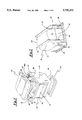
- FIG. 1 is a perspective view of the cassette with the cover and optional bottom aligned with the cassette.
- FIG. 2 is a perspective view of the semi-standard cassette showing an enclosed bottom and the H-bar side.
- FIG. 3 is a sectional view of the cassette of the type shown in FIG. 2, showing the inner side of the H-bar, with the alternate preferred indexing spheres shown.
- FIG. 3-A is a cross-sectional view through line A--A of FIG. 3.
- FIG. 4 is a sectional view of the cassette of the type shown in FIG. 1, with the cover and optional bottom engaged and a wafer positioned within the cassette.
- FIG. 4-B is a cross-sectional view through line B--B of FIG. 4, with the cover and bottom elevated from the cassette.
- FIG. 5 is a sectional end view of the cover of the type shown in FIG. 1, with the seal removed.
- FIG. 6 is an end view of the cover of the type shown in FIG. 1, with the seal removed.
- FIG. 7 is a perspective view of the cassette, showing the cover and optional bottom aligned with the cassette, a semi conductor wafer partially extending into the cassette and the optional handle and means for tracking, affixed to an end of the cassette.
- FIG. 1 there is indicated generally the sealable semiconductor wafer cassette 10, a cassette cover 24, a round, disk-shaped substrate or wafer 50, and an optional cassette bottom door 18.
- the semiconductor wafer cassette 10 has a chamber defined by a pair of opposing side walls 12 and 13, a pair of endwalls 14 and 16, an open top 20, and an optional open bottom 58.
- the cassette cover 24 is designed to close and seal the open top 20.
- the bottom door 18 is designed to close and seal the optional open bottom 58.
- the curved semiconductor wafer supporting sidewalls 12 and 13 extend downward from the two opposing perimeter lip edges 28 and 30 to the cassette bottom frame 26.
- a plurality of recess pairs 44a-t and 46a-t shaped like saw teeth with the apex of each recess pair aligned on opposing interior surfaces, best shown in FIGS. 1 and 3-A.
- Each recess pair forms a slot 45.
- the slots 45 formed by recessed pair 44a-t are likewise aligned with the slots formed by recessed pairs 46a-t to form a plurality of pairs of opposing slots.
- Each pair of opposing slots holds a substrate or wafer 50.
- the wafers 50 are also in perimeter contact with the lower portion of the curved sides 12 and 13.
- the inside of the optional bottom door 18 may be recessed to form a continuous support surface to the wafers 50 (see FIGS. 1 and 4).
- the cassette may be constructed with a varying number of recess pairs 44a-t and 46a-t to change the number of pairs of opposing slots without deviating from the invention.
- the end wall 14 forming an enclosed end of the semiconductor wafer cassette 10 has an optional processing handle 56 which extends relatively perpendicular to the end wall 14 and relatively parallel to the open top 20 (see FIG. 7).
- the cassette processing handle 56 forms a gripping surface.
- the optional cassette level tracking system 54 attached to the end wall 14 is the optional cassette level tracking system 54, allowing a semiconductor wafer cassette 10 to be tracked during processing, transportation, and storage.
- tracking systems including but not limited to: infrared encoders, radio frequency transmitters, and bar codes that interact with bar code readers.
- H-bar end 16 Opposite the end wall 14 is the H-bar end 16 that forms the other enclosed end of the semiconductor wafer cassette 10 (See FIG. 2).
- An H-bar 41 extends from the surface of the H-bar end that allows the cassette 10 to be indexed with the processing tool.
- an optional plurality of partial spheres 42 may extend from the H-bar end 16 allowing precise, consistent and reliable indexing.
- the optional partial spheres 42 form one surface of a three groove kinematic coupling.
- a three groove kinematic coupling consists of two kinematic coupling surfaces. Three spheres arranged to form a triangle are attached to one surface and three kinematic recesses or grooves, designed to align and engage the spheres, are formed within the other surface. The two surfaces are brought into contact. The spheres engage with the grooves, precisely orienting the two surfaces relative to the other. This coupling arrangement allows repeatability of the precise orientation of the two kinematic coupling surfaces and grooves.
- the preferred material for the spheres and grooves is a hard ceramic such as tungsten carbide, silicon nitride or zirconia. Of course other materials may also be used without deviating from the invention.
- Either the grooves or spheres may extend from the H-bar endwall 16, to form one kinematic coupling surface.
- the other surface is formed on a piece of equipment such as a process tool. This arrangement allows precise orientation between the cassette and the process tool so that the cassette opening is properly aligned with respect to the process tool.
- kinematic projections such as the partial spheres 42 of the kinematic coupling may replace the H-bar 41.
- Purging bores 53 extend through the H-bar end 16 at predetermined locations.
- a means for purging the cassette 10 consisting of a plurality of self sealing breather filters may extend from the end wall 16 centered over the purging bores 53, allowing the chamber of the sealed semiconductor wafer cassette 10 to be purged with particle-free air or an inert gas.
- a 0.02 micron filter polytetrafluoroethylene (PTFE) membrane is used. These filters may be sealed within a housing that in turn extends through and seals with the purging bore 53.
- Other suitable mechanisms can, of course, be used without deviating from the invention.
- the purging bores 53, optional handle 56, means for purging, and means for tracking 54 may alternatively be attached to the cover 24 or bottom 18 of the semiconductor wafer cassette without deviating from the invention.
- the open top 20 is formed by a perimeter lip 60, a perimeter shoulder 32 that extends perpendicularly downward from an inner edge of lip 60, and a ledge 34 that extends perpendicularly inward from the perimeter shoulder 32.
- the perimeter shoulder 32 and ledge 34 forms a first means for sealing the opening end of the cassette 10 (see FIG. 4).
- the perimeter lip 60 provides a support surface for stacking an inverted cassette that is compatable with SEMI standards.
- the cassette cover 24 is designed to close and seal the open top 20. Recessed around the perimeter of the cover 24 is a groove 82 that engages with a seal 23.
- the cover 24 When engaged, the cover 24 rests on the cassette perimeter ledge 34. Engaging the cover 24 with the semiconductor wafer cassette open end 20 engages the first and second means for sealing, thereby creating a hermetic seal.
- the cover may be constructed with a thickness about the same as the perimeter shoulder 32 so that when the cover 24 engages with the cassette 10, a relatively flat top surface is formed.
- the cover may also have a means for supporting the semiconductor wafers. This means for support may be positioned to align with the apex of each recess pair when the cover is engaged with the container. These supports would prevent movement of the wafer during transportation.
- the cover may be constructed to engage with other surfaces of the cassette, while still forming a hermetic seal without deviating from the invention.
- the present invention may be constructed with an enclosed bottom or with an open sealable bottom 58.
- cassette bottom inner shoulder 66 extends around the inside of the optional cassette bottom frame 26, forming a third sealing surface.
- the optional bottom door 18 has a seal 23 extending around the perimeter, forming a fourth sealing surface.
- FIGS. 1 and 2 Best shown in FIGS. 1 and 2 are four vertical edges 36 that form the corners of the semiconductor wafer cassette 10, providing rigidity and support to the cassette.
- the vertical edges 36 extend upward from the lower portion of each end of the curved sides 12 to the perimeter ledge 34.
- the mode of use will now be discussed.
- the operator of the wafer processing equipment indexes the sealed semiconductor wafer cassette 10 directly onto the processing tool.
- the processing equipment should provide a mini-environment that allows a slight overpressure within the mini-environment to prevent the exterior environment from entering into the clean mini-environment.
- the mini-environment must also provide good air flow to the processing tool.
- the cassette 10 may be indexed horizontally or vertically, depending on the preferred cassette orientation. Then, a processing tool with a suction and vacuum capability aligns and engages the cassette cover 24. The hermetic seal collapses allowing the process tool to remove the cover 24. Next, all the desired processes may be performed on the semiconductor wafers within the cassette. After all the desired processes have been performed, the cover 24 is then resealed by engaging the cover 24 with the cassette's perimeter ledge 34, discontinuing the vacuum and disengaging the suction. A hermetic seal is formed between the the perimeter shoulder 32, the ledge 34 and the cover's seal 23.
- the cassette may then be transported to other process stations, stored or otherwise transported.
- the cassette may be purged with an inert gas utilizing two 0.02 micron filter PTFE membranes providing a clean environment for substrates such as semiconductor wafers 50.
- the active purge is removed, the sealed cassette 10 will maintain the inert gas purge for several hours. This method allows the semiconductor wafers to be safely stored and transported in an unfriendly external environment.
- the optional tracking system 54 may be used to track the cassette in an external environment.
- the optional handle 56 on the endwall 14 of the cassette 10 facilitates loading and unloading a cassette into process equipment and storage areas.
Abstract
Description
Claims (13)
Priority Applications (1)
| Application Number | Priority Date | Filing Date | Title |
|---|---|---|---|
| US08/712,140 US5755332A (en) | 1994-03-11 | 1996-09-11 | Enclosed sealable purgible semiconductor wafer holder |
Applications Claiming Priority (3)
| Application Number | Priority Date | Filing Date | Title |
|---|---|---|---|
| US08/209,227 US5472086A (en) | 1994-03-11 | 1994-03-11 | Enclosed sealable purgible semiconductor wafer holder |
| US44795495A | 1995-05-23 | 1995-05-23 | |
| US08/712,140 US5755332A (en) | 1994-03-11 | 1996-09-11 | Enclosed sealable purgible semiconductor wafer holder |
Related Parent Applications (1)
| Application Number | Title | Priority Date | Filing Date |
|---|---|---|---|
| US44795495A Continuation | 1994-03-11 | 1995-05-23 |
Publications (1)
| Publication Number | Publication Date |
|---|---|
| US5755332A true US5755332A (en) | 1998-05-26 |
Family
ID=22777887
Family Applications (2)
| Application Number | Title | Priority Date | Filing Date |
|---|---|---|---|
| US08/209,227 Expired - Lifetime US5472086A (en) | 1994-03-11 | 1994-03-11 | Enclosed sealable purgible semiconductor wafer holder |
| US08/712,140 Expired - Lifetime US5755332A (en) | 1994-03-11 | 1996-09-11 | Enclosed sealable purgible semiconductor wafer holder |
Family Applications Before (1)
| Application Number | Title | Priority Date | Filing Date |
|---|---|---|---|
| US08/209,227 Expired - Lifetime US5472086A (en) | 1994-03-11 | 1994-03-11 | Enclosed sealable purgible semiconductor wafer holder |
Country Status (6)
| Country | Link |
|---|---|
| US (2) | US5472086A (en) |
| EP (1) | EP0749393B1 (en) |
| JP (1) | JP3202991B2 (en) |
| AT (1) | ATE256915T1 (en) |
| DE (1) | DE69433428T2 (en) |
| WO (1) | WO1995024348A1 (en) |
Cited By (30)
| Publication number | Priority date | Publication date | Assignee | Title |
|---|---|---|---|---|
| US6095335A (en) * | 1998-07-10 | 2000-08-01 | H-Square Corporation | Wafer support device having a retrofit to provide size convertibility |
| US6098809A (en) * | 1998-07-07 | 2000-08-08 | Shin-Etsu Polymer Co., Ltd. | Storage container for precision substrates |
| US6216874B1 (en) * | 1998-07-10 | 2001-04-17 | Fluoroware, Inc. | Wafer carrier having a low tolerance build-up |
| US6273261B1 (en) * | 1999-04-30 | 2001-08-14 | Shin-Etsu Polymer Co., Ltd. | Identification structure of a substrate storage container and method of identifying a substrate storage container |
| US6390145B1 (en) * | 1999-06-23 | 2002-05-21 | Tdk Corporation | Container and method for sealing the container |
| US6461437B1 (en) * | 2000-01-26 | 2002-10-08 | Mitsubishi Denki Kabushiki Kaisha | Apparatus used for fabricating liquid crystal device and method of fabricating the same |
| US6464081B2 (en) * | 1999-01-06 | 2002-10-15 | Entegris, Inc. | Door guide for a wafer container |
| US6536588B1 (en) | 1999-03-12 | 2003-03-25 | William Stephen Kyrwood | Golf club support |
| US20030089634A1 (en) * | 2001-11-15 | 2003-05-15 | Hugh Mason | Containment unit for protecting medical slides during transit |
| USRE38221E1 (en) | 1995-10-13 | 2003-08-19 | Entegris, Inc. | 300 mm microenvironment pod with door on side |
| US20030209404A1 (en) * | 2000-07-07 | 2003-11-13 | Davis Jeffry A. | Automated processing system |
| US6719142B1 (en) * | 2002-07-16 | 2004-04-13 | Ion Systems, Inc. | Apparatus and method for measuring static charge on wafers, disks, substrates, masks, and flat panel displays |
| US6723174B2 (en) | 1996-03-26 | 2004-04-20 | Semitool, Inc. | Automated semiconductor processing system |
| US6781205B1 (en) * | 2002-10-11 | 2004-08-24 | Ion Systems, Inc. | Electrostatic charge measurement on semiconductor wafers |
| US20040206664A1 (en) * | 1997-07-11 | 2004-10-21 | Entegris, Inc. | Transport module |
| US6817602B2 (en) | 2000-08-29 | 2004-11-16 | Freescale Semiconductor, Inc. | Manufacturing system method for processing a lithography mask container |
| US6833035B1 (en) * | 1994-04-28 | 2004-12-21 | Semitool, Inc. | Semiconductor processing system with wafer container docking and loading station |
| US6942738B1 (en) | 1996-07-15 | 2005-09-13 | Semitool, Inc. | Automated semiconductor processing system |
| US20050224391A1 (en) * | 2001-11-27 | 2005-10-13 | Gregory Bores | Front opening wafer carrier with path to ground effectuated by door |
| US20060076253A1 (en) * | 2004-10-08 | 2006-04-13 | Maxtor Corporation | Container for disk drives |
| US20060207916A1 (en) * | 2003-03-04 | 2006-09-21 | Shin-Etsu Polymer Co.,Ltd | Precision substrate storage container |
| US7175026B2 (en) | 2002-05-03 | 2007-02-13 | Maxtor Corporation | Memory disk shipping container with improved contaminant control |
| US20070118300A1 (en) * | 2005-11-18 | 2007-05-24 | Texas Instruments Incorporated | Method and apparatus for cassette integrity testing using a wafer sorter |
| US20070187268A1 (en) * | 2006-02-10 | 2007-08-16 | Maxtor Corporation | Container for Consumer Electronics |
| SG136846A1 (en) * | 2006-04-27 | 2007-11-29 | Ssr Mfg Corp | Apparatus for opening/closing cover of thin-film disc containing cassette |
| US20080017547A1 (en) * | 2003-11-07 | 2008-01-24 | Entegris, Inc. | Front opening substrate container with bottom plate |
| US20080302700A1 (en) * | 1997-07-11 | 2008-12-11 | Nyseth David L | Transport module |
| US20100163452A1 (en) * | 2008-12-26 | 2010-07-01 | Chin-Ming Lin | Wafer container having the purging valve |
| US20100175781A1 (en) * | 2007-07-09 | 2010-07-15 | Kondoh Industries, Ltd. | Apparatus for Charging Dry Air or Nitrogen Gas into a Container for Storing Semiconductor Wafers and an Apparatus for Thereby Removing Static Electricity from the Wafers |
| WO2012151431A2 (en) | 2011-05-03 | 2012-11-08 | Entergris, Inc. | Wafer container with particle shield |
Families Citing this family (26)
| Publication number | Priority date | Publication date | Assignee | Title |
|---|---|---|---|---|
| US5472086A (en) * | 1994-03-11 | 1995-12-05 | Holliday; James E. | Enclosed sealable purgible semiconductor wafer holder |
| JP3257328B2 (en) * | 1995-03-16 | 2002-02-18 | 株式会社日立製作所 | Plasma processing apparatus and plasma processing method |
| KR960043084A (en) * | 1995-05-22 | 1996-12-23 | 웨인 피이 베일리 | Single structure fud and cassette assemblies |
| US5833726A (en) * | 1995-05-26 | 1998-11-10 | Extraction System, Inc. | Storing substrates between process steps within a processing facility |
| USD378873S (en) * | 1995-10-13 | 1997-04-22 | Empak, Inc. | 300 mm microenvironment pod with door on side |
| USD383898S (en) * | 1995-10-13 | 1997-09-23 | Empak, Inc. | Combination shipping and transport cassette |
| USD387903S (en) * | 1995-10-13 | 1997-12-23 | Empak, Inc. | Shipping container |
| US5873468A (en) * | 1995-11-16 | 1999-02-23 | Sumitomo Sitix Corporation | Thin-plate supporting container with filter means |
| US6003674A (en) * | 1996-05-13 | 1999-12-21 | Brooks; Ray Gene | Method and apparatus for packing contaminant-sensitive articles and resulting package |
| US5724748A (en) * | 1996-07-24 | 1998-03-10 | Brooks; Ray G. | Apparatus for packaging contaminant-sensitive articles and resulting package |
| US5921397A (en) * | 1996-12-10 | 1999-07-13 | Empak, Inc. | Disk cassette |
| US5833067A (en) * | 1997-03-10 | 1998-11-10 | Seagate Technologies, Inc. | Disk caddy and lid with barrier means |
| US6076585A (en) * | 1998-03-02 | 2000-06-20 | Motorola, Inc. | Method of manufacturing a semiconductor device and apparatus therefor |
| JP3656701B2 (en) * | 1998-03-23 | 2005-06-08 | 東京エレクトロン株式会社 | Processing equipment |
| US6267245B1 (en) | 1998-07-10 | 2001-07-31 | Fluoroware, Inc. | Cushioned wafer container |
| US6168364B1 (en) * | 1999-04-19 | 2001-01-02 | Tdk Corporation | Vacuum clean box, clean transfer method and apparatus therefor |
| US6561894B1 (en) | 1999-04-19 | 2003-05-13 | Tdk Corporation | Clean box, clean transfer method and apparatus therefor |
| CN1128470C (en) | 2000-09-01 | 2003-11-19 | 陈正明 | Bulk production process of thinned wafer separated from carrier and its equipment |
| JP4128811B2 (en) * | 2001-08-10 | 2008-07-30 | 株式会社トプコン | Surface inspection device |
| US7252199B2 (en) * | 2004-03-26 | 2007-08-07 | Entegris, Inc. | Disk cassette system |
| US20080019811A1 (en) * | 2006-07-11 | 2008-01-24 | Michael Krolak | Method and apparatus for vertical wafer transport, buffer and storage |
| US20100020440A1 (en) * | 2008-07-25 | 2010-01-28 | Seagate Technology Llc | Low profile substrate shipper |
| US20120288355A1 (en) * | 2011-05-11 | 2012-11-15 | Ming-Teng Hsieh | Method for storing wafers |
| JP5888288B2 (en) * | 2013-06-26 | 2016-03-16 | 株式会社ダイフク | Inspection equipment for goods storage facilities |
| US10566226B2 (en) * | 2014-11-11 | 2020-02-18 | Applied Materials, Inc. | Multi-cassette carrying case |
| JP6451453B2 (en) * | 2015-03-31 | 2019-01-16 | Tdk株式会社 | GAS PURGE DEVICE, LOAD PORT DEVICE, PURGE CONTAINER CONTAINER STAND, AND GAS PURGE METHOD |
Citations (53)
| Publication number | Priority date | Publication date | Assignee | Title |
|---|---|---|---|---|
| US3913749A (en) * | 1974-08-12 | 1975-10-21 | Fluoroware Systems Corp | Wafer basket transfer apparatus |
| US3918756A (en) * | 1973-12-26 | 1975-11-11 | Fluoroware Inc | Wafer holder |
| US3923191A (en) * | 1974-09-11 | 1975-12-02 | Fluoroware Inc | Wafer basket and handle |
| US3923156A (en) * | 1974-04-29 | 1975-12-02 | Fluoroware Inc | Wafer basket |
| US3926305A (en) * | 1973-07-12 | 1975-12-16 | Fluoroware Inc | Wafer basket |
| US3939973A (en) * | 1974-01-14 | 1976-02-24 | Fluoroware, Inc. | Wafer basket and easily attached and detached carrier for same |
| US3961877A (en) * | 1974-09-11 | 1976-06-08 | Fluoroware, Inc. | Reinforced wafer basket |
| US4043451A (en) * | 1976-03-18 | 1977-08-23 | Fluoroware, Inc. | Shipping container for silicone semiconductor wafers |
| US4061228A (en) * | 1976-12-20 | 1977-12-06 | Fluoroware, Inc. | Shipping container for substrates |
| US4248346A (en) * | 1979-01-29 | 1981-02-03 | Fluoroware, Inc. | Shipping container for semiconductor substrate wafers |
| US4450960A (en) * | 1982-08-30 | 1984-05-29 | Empak Inc. | Package |
| US4471716A (en) * | 1981-01-15 | 1984-09-18 | Fluoroware, Inc. | Wafer carrier |
| US4520925A (en) * | 1983-08-09 | 1985-06-04 | Empak Inc. | Package |
| US4532970A (en) * | 1983-09-28 | 1985-08-06 | Hewlett-Packard Company | Particle-free dockable interface for integrated circuit processing |
| US4543389A (en) * | 1984-04-10 | 1985-09-24 | Shell Oil Company | Copolymerization catalyst and process for polymerizing impact resistant ethylene-propylene polymers |
| US4555024A (en) * | 1984-04-12 | 1985-11-26 | Wacker-Chemie Gmbh | Packaging unit for semiconductor wafers |
| US4557382A (en) * | 1983-08-17 | 1985-12-10 | Empak Inc. | Disk package |
| US4588086A (en) * | 1984-06-07 | 1986-05-13 | Coe Thomas U | Substrate and media carrier |
| US4684021A (en) * | 1986-06-23 | 1987-08-04 | Fluoroware, Inc. | Bottom loading wafer carrier box |
| US4718549A (en) * | 1985-03-08 | 1988-01-12 | Dynamit Nobel Silicon S.P.A. | Container for the storage and shipment of silicon disks or wafers |
| US4718552A (en) * | 1986-12-11 | 1988-01-12 | Fluoroware, Inc. | Disk shipper and transfer tray |
| US4721207A (en) * | 1986-04-28 | 1988-01-26 | Tensho Electric Industrial Co., Ltd. | Hard disk container |
| US4739882A (en) * | 1986-02-13 | 1988-04-26 | Asyst Technologies | Container having disposable liners |
| US4747488A (en) * | 1986-12-01 | 1988-05-31 | Shoji Kikuchi | Hard disk container |
| US4752007A (en) * | 1986-12-11 | 1988-06-21 | Fluoroware, Inc. | Disk shipper |
| US4793488A (en) * | 1987-07-07 | 1988-12-27 | Empak, Inc. | Package for semiconductor wafers |
| US4815912A (en) * | 1984-12-24 | 1989-03-28 | Asyst Technologies, Inc. | Box door actuated retainer |
| US4817795A (en) * | 1988-03-04 | 1989-04-04 | Fluoroware, Inc. | Robotic accessible wafer shipper assembly |
| US4817799A (en) * | 1986-10-06 | 1989-04-04 | Empak, Inc. | Disk package |
| US4827110A (en) * | 1987-06-11 | 1989-05-02 | Fluoroware, Inc. | Method and apparatus for monitoring the location of wafer disks |
| US4833306A (en) * | 1988-05-18 | 1989-05-23 | Fluoroware, Inc. | Bar code remote recognition system for process carriers of wafer disks |
| US4872554A (en) * | 1987-07-02 | 1989-10-10 | Fluoroware, Inc. | Reinforced carrier with embedded rigid insert |
| US4880116A (en) * | 1988-03-04 | 1989-11-14 | Fluoroware, Inc. | Robotic accessible wafer shipper assembly |
| US4930634A (en) * | 1987-09-29 | 1990-06-05 | Fluoroware, Inc. | Carrier for flat panel displays |
| US4949848A (en) * | 1988-04-29 | 1990-08-21 | Fluoroware, Inc. | Wafer carrier |
| USRE33361E (en) * | 1984-06-07 | 1990-10-02 | Substrate and media carrier | |
| US4966284A (en) * | 1987-07-07 | 1990-10-30 | Empak, Inc. | Substrate package |
| US4966519A (en) * | 1985-10-24 | 1990-10-30 | Texas Instruments Incorporated | Integrated circuit processing system |
| US4995430A (en) * | 1989-05-19 | 1991-02-26 | Asyst Technologies, Inc. | Sealable transportable container having improved latch mechanism |
| US5024329A (en) * | 1988-04-22 | 1991-06-18 | Siemens Aktiengesellschaft | Lockable container for transporting and for storing semiconductor wafers |
| US5025926A (en) * | 1987-07-07 | 1991-06-25 | Empak, Inc. | Package |
| US5046615A (en) * | 1989-04-03 | 1991-09-10 | Fluoroware, Inc. | Disk shipper |
| US5111936A (en) * | 1990-11-30 | 1992-05-12 | Fluoroware | Wafer carrier |
| WO1992016964A1 (en) * | 1991-03-20 | 1992-10-01 | Fluoroware Inc | Cushioned cover for wafer container |
| US5154301A (en) * | 1991-09-12 | 1992-10-13 | Fluoroware, Inc. | Wafer carrier |
| US5184723A (en) * | 1991-05-14 | 1993-02-09 | Fluoroware, Inc. | Single wafer robotic package |
| US5207324A (en) * | 1991-03-08 | 1993-05-04 | Fluoroware, Inc. | Wafer cushion for shippers |
| US5217053A (en) * | 1990-02-05 | 1993-06-08 | Texas Instruments Incorporated | Vented vacuum semiconductor wafer cassette |
| US5228568A (en) * | 1991-08-30 | 1993-07-20 | Shin-Etsu Handotai Co., Ltd. | Semiconductor wafer basket |
| US5255797A (en) * | 1992-02-26 | 1993-10-26 | Fluoroware, Inc. | Wafer carrier with wafer retaining cushions |
| US5255783A (en) * | 1991-12-20 | 1993-10-26 | Fluoroware, Inc. | Evacuated wafer container |
| US5295522A (en) * | 1992-09-24 | 1994-03-22 | International Business Machines Corporation | Gas purge system for isolation enclosure for contamination sensitive items |
| US5472086A (en) * | 1994-03-11 | 1995-12-05 | Holliday; James E. | Enclosed sealable purgible semiconductor wafer holder |
Family Cites Families (1)
| Publication number | Priority date | Publication date | Assignee | Title |
|---|---|---|---|---|
| US5137063A (en) * | 1990-02-05 | 1992-08-11 | Texas Instruments Incorporated | Vented vacuum semiconductor wafer cassette |
-
1994
- 1994-03-11 US US08/209,227 patent/US5472086A/en not_active Expired - Lifetime
- 1994-06-29 WO PCT/US1994/007357 patent/WO1995024348A1/en active IP Right Grant
- 1994-06-29 DE DE69433428T patent/DE69433428T2/en not_active Expired - Lifetime
- 1994-06-29 AT AT94922053T patent/ATE256915T1/en not_active IP Right Cessation
- 1994-06-29 JP JP52342795A patent/JP3202991B2/en not_active Expired - Lifetime
- 1994-06-29 EP EP94922053A patent/EP0749393B1/en not_active Expired - Lifetime
-
1996
- 1996-09-11 US US08/712,140 patent/US5755332A/en not_active Expired - Lifetime
Patent Citations (57)
| Publication number | Priority date | Publication date | Assignee | Title |
|---|---|---|---|---|
| US3926305A (en) * | 1973-07-12 | 1975-12-16 | Fluoroware Inc | Wafer basket |
| US3918756A (en) * | 1973-12-26 | 1975-11-11 | Fluoroware Inc | Wafer holder |
| US3939973A (en) * | 1974-01-14 | 1976-02-24 | Fluoroware, Inc. | Wafer basket and easily attached and detached carrier for same |
| US3923156A (en) * | 1974-04-29 | 1975-12-02 | Fluoroware Inc | Wafer basket |
| US3913749A (en) * | 1974-08-12 | 1975-10-21 | Fluoroware Systems Corp | Wafer basket transfer apparatus |
| US3961877A (en) * | 1974-09-11 | 1976-06-08 | Fluoroware, Inc. | Reinforced wafer basket |
| US3961877B1 (en) * | 1974-09-11 | 1987-11-03 | ||
| US3923191A (en) * | 1974-09-11 | 1975-12-02 | Fluoroware Inc | Wafer basket and handle |
| US4043451A (en) * | 1976-03-18 | 1977-08-23 | Fluoroware, Inc. | Shipping container for silicone semiconductor wafers |
| US4061228A (en) * | 1976-12-20 | 1977-12-06 | Fluoroware, Inc. | Shipping container for substrates |
| US4248346A (en) * | 1979-01-29 | 1981-02-03 | Fluoroware, Inc. | Shipping container for semiconductor substrate wafers |
| US4471716A (en) * | 1981-01-15 | 1984-09-18 | Fluoroware, Inc. | Wafer carrier |
| US4450960A (en) * | 1982-08-30 | 1984-05-29 | Empak Inc. | Package |
| US4520925A (en) * | 1983-08-09 | 1985-06-04 | Empak Inc. | Package |
| US4557382A (en) * | 1983-08-17 | 1985-12-10 | Empak Inc. | Disk package |
| US4532970A (en) * | 1983-09-28 | 1985-08-06 | Hewlett-Packard Company | Particle-free dockable interface for integrated circuit processing |
| US4543389A (en) * | 1984-04-10 | 1985-09-24 | Shell Oil Company | Copolymerization catalyst and process for polymerizing impact resistant ethylene-propylene polymers |
| US4555024A (en) * | 1984-04-12 | 1985-11-26 | Wacker-Chemie Gmbh | Packaging unit for semiconductor wafers |
| US4588086A (en) * | 1984-06-07 | 1986-05-13 | Coe Thomas U | Substrate and media carrier |
| USRE33361E (en) * | 1984-06-07 | 1990-10-02 | Substrate and media carrier | |
| US4815912A (en) * | 1984-12-24 | 1989-03-28 | Asyst Technologies, Inc. | Box door actuated retainer |
| US4718549A (en) * | 1985-03-08 | 1988-01-12 | Dynamit Nobel Silicon S.P.A. | Container for the storage and shipment of silicon disks or wafers |
| US4966519A (en) * | 1985-10-24 | 1990-10-30 | Texas Instruments Incorporated | Integrated circuit processing system |
| US4739882A (en) * | 1986-02-13 | 1988-04-26 | Asyst Technologies | Container having disposable liners |
| US4721207A (en) * | 1986-04-28 | 1988-01-26 | Tensho Electric Industrial Co., Ltd. | Hard disk container |
| US4684021A (en) * | 1986-06-23 | 1987-08-04 | Fluoroware, Inc. | Bottom loading wafer carrier box |
| US4817799A (en) * | 1986-10-06 | 1989-04-04 | Empak, Inc. | Disk package |
| US4747488A (en) * | 1986-12-01 | 1988-05-31 | Shoji Kikuchi | Hard disk container |
| US4718552A (en) * | 1986-12-11 | 1988-01-12 | Fluoroware, Inc. | Disk shipper and transfer tray |
| US4752007A (en) * | 1986-12-11 | 1988-06-21 | Fluoroware, Inc. | Disk shipper |
| US4888473A (en) * | 1987-06-11 | 1989-12-19 | Fluoroware, Inc. | Wafer disk location monitoring system and tagged process carriers for use therewith |
| US4827110A (en) * | 1987-06-11 | 1989-05-02 | Fluoroware, Inc. | Method and apparatus for monitoring the location of wafer disks |
| US4888473B1 (en) * | 1987-06-11 | 1996-10-15 | Fluoroware Inc | Wafer disk location monitoring system and tagged process carrier for use therewith |
| US4872554A (en) * | 1987-07-02 | 1989-10-10 | Fluoroware, Inc. | Reinforced carrier with embedded rigid insert |
| US5025926A (en) * | 1987-07-07 | 1991-06-25 | Empak, Inc. | Package |
| US4793488A (en) * | 1987-07-07 | 1988-12-27 | Empak, Inc. | Package for semiconductor wafers |
| US4966284A (en) * | 1987-07-07 | 1990-10-30 | Empak, Inc. | Substrate package |
| US4930634A (en) * | 1987-09-29 | 1990-06-05 | Fluoroware, Inc. | Carrier for flat panel displays |
| US4880116A (en) * | 1988-03-04 | 1989-11-14 | Fluoroware, Inc. | Robotic accessible wafer shipper assembly |
| US4817795A (en) * | 1988-03-04 | 1989-04-04 | Fluoroware, Inc. | Robotic accessible wafer shipper assembly |
| US5024329A (en) * | 1988-04-22 | 1991-06-18 | Siemens Aktiengesellschaft | Lockable container for transporting and for storing semiconductor wafers |
| US4949848A (en) * | 1988-04-29 | 1990-08-21 | Fluoroware, Inc. | Wafer carrier |
| US4833306A (en) * | 1988-05-18 | 1989-05-23 | Fluoroware, Inc. | Bar code remote recognition system for process carriers of wafer disks |
| US5046615A (en) * | 1989-04-03 | 1991-09-10 | Fluoroware, Inc. | Disk shipper |
| US4995430A (en) * | 1989-05-19 | 1991-02-26 | Asyst Technologies, Inc. | Sealable transportable container having improved latch mechanism |
| US5217053A (en) * | 1990-02-05 | 1993-06-08 | Texas Instruments Incorporated | Vented vacuum semiconductor wafer cassette |
| US5111936A (en) * | 1990-11-30 | 1992-05-12 | Fluoroware | Wafer carrier |
| US5207324A (en) * | 1991-03-08 | 1993-05-04 | Fluoroware, Inc. | Wafer cushion for shippers |
| WO1992016964A1 (en) * | 1991-03-20 | 1992-10-01 | Fluoroware Inc | Cushioned cover for wafer container |
| US5253755A (en) * | 1991-03-20 | 1993-10-19 | Fluoroware, Inc. | Cushioned cover for disk container |
| US5184723A (en) * | 1991-05-14 | 1993-02-09 | Fluoroware, Inc. | Single wafer robotic package |
| US5228568A (en) * | 1991-08-30 | 1993-07-20 | Shin-Etsu Handotai Co., Ltd. | Semiconductor wafer basket |
| US5154301A (en) * | 1991-09-12 | 1992-10-13 | Fluoroware, Inc. | Wafer carrier |
| US5255783A (en) * | 1991-12-20 | 1993-10-26 | Fluoroware, Inc. | Evacuated wafer container |
| US5255797A (en) * | 1992-02-26 | 1993-10-26 | Fluoroware, Inc. | Wafer carrier with wafer retaining cushions |
| US5295522A (en) * | 1992-09-24 | 1994-03-22 | International Business Machines Corporation | Gas purge system for isolation enclosure for contamination sensitive items |
| US5472086A (en) * | 1994-03-11 | 1995-12-05 | Holliday; James E. | Enclosed sealable purgible semiconductor wafer holder |
Non-Patent Citations (2)
| Title |
|---|
| Slocum, Alexander H., "Sematech Short Course: Determinatistic Machine Design Increasing Reliability and Performance", Precision Machine Design, Prentice Hall, Englewood Cliffs, 1992, pp. 49-64. |
| Slocum, Alexander H., Sematech Short Course: Determinatistic Machine Design Increasing Reliability and Performance , Precision Machine Design , Prentice Hall, Englewood Cliffs, 1992, pp. 49 64. * |
Cited By (45)
| Publication number | Priority date | Publication date | Assignee | Title |
|---|---|---|---|---|
| US6833035B1 (en) * | 1994-04-28 | 2004-12-21 | Semitool, Inc. | Semiconductor processing system with wafer container docking and loading station |
| USRE38221E1 (en) | 1995-10-13 | 2003-08-19 | Entegris, Inc. | 300 mm microenvironment pod with door on side |
| USRE42402E1 (en) | 1995-10-13 | 2011-05-31 | Entegris, Inc. | 300 mm microenvironment pod with door on side |
| USRE41231E1 (en) | 1995-10-13 | 2010-04-20 | Entegris, Inc. | 300 mm microenvironment pod with door on side |
| US6723174B2 (en) | 1996-03-26 | 2004-04-20 | Semitool, Inc. | Automated semiconductor processing system |
| US6942738B1 (en) | 1996-07-15 | 2005-09-13 | Semitool, Inc. | Automated semiconductor processing system |
| US20040206664A1 (en) * | 1997-07-11 | 2004-10-21 | Entegris, Inc. | Transport module |
| US20080302700A1 (en) * | 1997-07-11 | 2008-12-11 | Nyseth David L | Transport module |
| US7370764B2 (en) * | 1997-07-11 | 2008-05-13 | Entegris, Inc. | Transport module |
| US6098809A (en) * | 1998-07-07 | 2000-08-08 | Shin-Etsu Polymer Co., Ltd. | Storage container for precision substrates |
| US6520338B2 (en) * | 1998-07-10 | 2003-02-18 | Entegris, Inc. | Wafer carrier having a low tolerance build-up |
| US6095335A (en) * | 1998-07-10 | 2000-08-01 | H-Square Corporation | Wafer support device having a retrofit to provide size convertibility |
| US6216874B1 (en) * | 1998-07-10 | 2001-04-17 | Fluoroware, Inc. | Wafer carrier having a low tolerance build-up |
| US6464081B2 (en) * | 1999-01-06 | 2002-10-15 | Entegris, Inc. | Door guide for a wafer container |
| US6536588B1 (en) | 1999-03-12 | 2003-03-25 | William Stephen Kyrwood | Golf club support |
| US6273261B1 (en) * | 1999-04-30 | 2001-08-14 | Shin-Etsu Polymer Co., Ltd. | Identification structure of a substrate storage container and method of identifying a substrate storage container |
| US6390145B1 (en) * | 1999-06-23 | 2002-05-21 | Tdk Corporation | Container and method for sealing the container |
| US6461437B1 (en) * | 2000-01-26 | 2002-10-08 | Mitsubishi Denki Kabushiki Kaisha | Apparatus used for fabricating liquid crystal device and method of fabricating the same |
| US7278813B2 (en) | 2000-07-07 | 2007-10-09 | Semitool, Inc. | Automated processing system |
| US20030209404A1 (en) * | 2000-07-07 | 2003-11-13 | Davis Jeffry A. | Automated processing system |
| US6817602B2 (en) | 2000-08-29 | 2004-11-16 | Freescale Semiconductor, Inc. | Manufacturing system method for processing a lithography mask container |
| US6866150B2 (en) * | 2001-11-15 | 2005-03-15 | The Mason Box Company, Inc. | Containment unit for protecting medical slides during transit |
| US20030089634A1 (en) * | 2001-11-15 | 2003-05-15 | Hugh Mason | Containment unit for protecting medical slides during transit |
| US8276759B2 (en) | 2001-11-27 | 2012-10-02 | Entegris, Inc. | Front opening wafer carrier with path to ground effectuated by door |
| US20110131800A1 (en) * | 2001-11-27 | 2011-06-09 | Entegris, Inc. | Front opening wafer contaner with path to ground effectuated by door |
| US20050224391A1 (en) * | 2001-11-27 | 2005-10-13 | Gregory Bores | Front opening wafer carrier with path to ground effectuated by door |
| US7886910B2 (en) | 2001-11-27 | 2011-02-15 | Entegris, Inc. | Front opening wafer carrier with path to ground effectuated by door |
| US7175026B2 (en) | 2002-05-03 | 2007-02-13 | Maxtor Corporation | Memory disk shipping container with improved contaminant control |
| US6719142B1 (en) * | 2002-07-16 | 2004-04-13 | Ion Systems, Inc. | Apparatus and method for measuring static charge on wafers, disks, substrates, masks, and flat panel displays |
| US6781205B1 (en) * | 2002-10-11 | 2004-08-24 | Ion Systems, Inc. | Electrostatic charge measurement on semiconductor wafers |
| US20060207916A1 (en) * | 2003-03-04 | 2006-09-21 | Shin-Etsu Polymer Co.,Ltd | Precision substrate storage container |
| US7523829B2 (en) | 2003-03-04 | 2009-04-28 | Shin-Etsu Polymer Co., Ltd. | Precision substrate storage container |
| US7866480B2 (en) * | 2003-11-07 | 2011-01-11 | Entegris, Inc. | Front opening substrate container with bottom plate |
| US20080017547A1 (en) * | 2003-11-07 | 2008-01-24 | Entegris, Inc. | Front opening substrate container with bottom plate |
| US7584851B2 (en) | 2004-10-08 | 2009-09-08 | Seagate Technology Llc | Container for disk drives |
| US20060076253A1 (en) * | 2004-10-08 | 2006-04-13 | Maxtor Corporation | Container for disk drives |
| US7596456B2 (en) | 2005-11-18 | 2009-09-29 | Texas Instruments Incorporated | Method and apparatus for cassette integrity testing using a wafer sorter |
| US20070118300A1 (en) * | 2005-11-18 | 2007-05-24 | Texas Instruments Incorporated | Method and apparatus for cassette integrity testing using a wafer sorter |
| US7810639B2 (en) | 2006-02-10 | 2010-10-12 | Seagate Technology Llc | Container for consumer electronics |
| US20070187268A1 (en) * | 2006-02-10 | 2007-08-16 | Maxtor Corporation | Container for Consumer Electronics |
| SG136846A1 (en) * | 2006-04-27 | 2007-11-29 | Ssr Mfg Corp | Apparatus for opening/closing cover of thin-film disc containing cassette |
| US20100175781A1 (en) * | 2007-07-09 | 2010-07-15 | Kondoh Industries, Ltd. | Apparatus for Charging Dry Air or Nitrogen Gas into a Container for Storing Semiconductor Wafers and an Apparatus for Thereby Removing Static Electricity from the Wafers |
| US7950524B2 (en) * | 2008-12-26 | 2011-05-31 | Gudeng Precision Industrial Co., Ltd | Wafer container having the purging valve |
| US20100163452A1 (en) * | 2008-12-26 | 2010-07-01 | Chin-Ming Lin | Wafer container having the purging valve |
| WO2012151431A2 (en) | 2011-05-03 | 2012-11-08 | Entergris, Inc. | Wafer container with particle shield |
Also Published As
| Publication number | Publication date |
|---|---|
| EP0749393A1 (en) | 1996-12-27 |
| DE69433428D1 (en) | 2004-01-29 |
| JP3202991B2 (en) | 2001-08-27 |
| EP0749393A4 (en) | 1997-07-02 |
| WO1995024348A1 (en) | 1995-09-14 |
| US5472086A (en) | 1995-12-05 |
| JPH09507726A (en) | 1997-08-05 |
| DE69433428T2 (en) | 2004-10-07 |
| EP0749393B1 (en) | 2003-12-17 |
| ATE256915T1 (en) | 2004-01-15 |
Similar Documents
| Publication | Publication Date | Title |
|---|---|---|
| US5755332A (en) | Enclosed sealable purgible semiconductor wafer holder | |
| US5476176A (en) | Reinforced semiconductor wafer holder | |
| US5697750A (en) | Controlled environment enclosure and mechanical interface | |
| KR100347203B1 (en) | Enclosure for load lock interface | |
| US5586585A (en) | Direct loadlock interface | |
| US5944857A (en) | Multiple single-wafer loadlock wafer processing apparatus and loading and unloading method therefor | |
| US6696367B1 (en) | System for the improved handling of wafers within a process tool | |
| JP2644166B2 (en) | Pressurized sealed portable container | |
| EP0555891B1 (en) | Vacuum processing system and method | |
| US5044871A (en) | Integrated circuit processing system | |
| JP2644167B2 (en) | Computerized conveyor based manufacturing line structure. | |
| EP0582018B1 (en) | Pressurized interface apparatus for transferring a semiconductor wafer between a pressurized sealable transportable container and a processing equipment | |
| JPH0774227A (en) | Load lock under microenvironment | |
| EP0582017A1 (en) | Dispatching apparatus with a gas supply distribution system for handling and storing pressurized sealable transportable containers | |
| US20160141189A1 (en) | Frame cassette | |
| US20210296149A1 (en) | Enclosure system shelf | |
| JP2002517088A (en) | Batch type end effector for semiconductor wafer handling | |
| EP1119039A1 (en) | Wafer storing method and storing container therefor and wafer transferring method for transferring wafer to the storing container | |
| JP2757102B2 (en) | Clean transfer method and device | |
| US4943457A (en) | Vacuum slice carrier | |
| EP0818806A2 (en) | Method and apparatus for transporting and using a semiconductor substrate carrier | |
| EP0744765A1 (en) | Apparatus for storing and carrying semiconductor wafers | |
| US11195735B2 (en) | Load lock for a substrate container and device having such a load lock | |
| KR100335815B1 (en) | Sealable, washable semiconductor wafer holder | |
| KR100292065B1 (en) | Standard mechanical interface system having function for eliminating contamination particle |
Legal Events
| Date | Code | Title | Description |
|---|---|---|---|
| STCF | Information on status: patent grant |
Free format text: PATENTED CASE |
|
| FPAY | Fee payment |
Year of fee payment: 4 |
|
| FPAY | Fee payment |
Year of fee payment: 8 |
|
| AS | Assignment |
Owner name: WELLS FARGO BANK, NATIONAL ASSOCIATION, AS AGENT, Free format text: SECURITY AGREEMENT;ASSIGNOR:ENTEGRIS, INC.;REEL/FRAME:022354/0784 Effective date: 20090302 Owner name: WELLS FARGO BANK, NATIONAL ASSOCIATION, AS AGENT,M Free format text: SECURITY AGREEMENT;ASSIGNOR:ENTEGRIS, INC.;REEL/FRAME:022354/0784 Effective date: 20090302 |
|
| FPAY | Fee payment |
Year of fee payment: 12 |
|
| AS | Assignment |
Owner name: ENTEGRIS, INC., MASSACHUSETTS Free format text: RELEASE BY SECURED PARTY;ASSIGNOR:WELLS FARGO BANK NATIONAL ASSOCIATION;REEL/FRAME:026764/0880 Effective date: 20110609 |
|
| AS | Assignment |
Owner name: GOLDMAN SACHS BANK USA, AS COLLATERAL AGENT, NEW YORK Free format text: SECURITY INTEREST;ASSIGNORS:ENTEGRIS, INC.;POCO GRAPHITE, INC.;ATMI, INC.;AND OTHERS;REEL/FRAME:032815/0852 Effective date: 20140430 Owner name: GOLDMAN SACHS BANK USA, AS COLLATERAL AGENT, NEW Y Free format text: SECURITY INTEREST;ASSIGNORS:ENTEGRIS, INC.;POCO GRAPHITE, INC.;ATMI, INC.;AND OTHERS;REEL/FRAME:032815/0852 Effective date: 20140430 |
|
| AS | Assignment |
Owner name: GOLDMAN SACHS BANK USA, AS COLLATERAL AGENT, NEW YORK Free format text: SECURITY INTEREST;ASSIGNORS:ENTEGRIS, INC.;POCO GRAPHITE, INC.;ATMI, INC.;AND OTHERS;REEL/FRAME:032812/0192 Effective date: 20140430 Owner name: GOLDMAN SACHS BANK USA, AS COLLATERAL AGENT, NEW Y Free format text: SECURITY INTEREST;ASSIGNORS:ENTEGRIS, INC.;POCO GRAPHITE, INC.;ATMI, INC.;AND OTHERS;REEL/FRAME:032812/0192 Effective date: 20140430 |
|
| AS | Assignment |
Owner name: ENTEGRIS, INC., MASSACHUSETTS Free format text: RELEASE BY SECURED PARTY;ASSIGNOR:GOLDMAN SACHS BANK USA, AS COLLATERAL AGENT;REEL/FRAME:047477/0032 Effective date: 20181106 Owner name: POCO GRAPHITE, INC., MASSACHUSETTS Free format text: RELEASE BY SECURED PARTY;ASSIGNOR:GOLDMAN SACHS BANK USA, AS COLLATERAL AGENT;REEL/FRAME:047477/0032 Effective date: 20181106 Owner name: ADVANCED TECHNOLOGY MATERIALS, INC., CONNECTICUT Free format text: RELEASE BY SECURED PARTY;ASSIGNOR:GOLDMAN SACHS BANK USA, AS COLLATERAL AGENT;REEL/FRAME:047477/0032 Effective date: 20181106 Owner name: ATMI, INC., CONNECTICUT Free format text: RELEASE BY SECURED PARTY;ASSIGNOR:GOLDMAN SACHS BANK USA, AS COLLATERAL AGENT;REEL/FRAME:047477/0032 Effective date: 20181106 Owner name: ATMI PACKAGING, INC., CONNECTICUT Free format text: RELEASE BY SECURED PARTY;ASSIGNOR:GOLDMAN SACHS BANK USA, AS COLLATERAL AGENT;REEL/FRAME:047477/0032 Effective date: 20181106 Owner name: ENTEGRIS, INC., MASSACHUSETTS Free format text: RELEASE BY SECURED PARTY;ASSIGNOR:GOLDMAN SACHS BANK USA, AS COLLATERAL AGENT;REEL/FRAME:047477/0151 Effective date: 20181106 Owner name: ATMI PACKAGING, INC., CONNECTICUT Free format text: RELEASE BY SECURED PARTY;ASSIGNOR:GOLDMAN SACHS BANK USA, AS COLLATERAL AGENT;REEL/FRAME:047477/0151 Effective date: 20181106 Owner name: ADVANCED TECHNOLOGY MATERIALS, INC., CONNECTICUT Free format text: RELEASE BY SECURED PARTY;ASSIGNOR:GOLDMAN SACHS BANK USA, AS COLLATERAL AGENT;REEL/FRAME:047477/0151 Effective date: 20181106 Owner name: ATMI, INC., CONNECTICUT Free format text: RELEASE BY SECURED PARTY;ASSIGNOR:GOLDMAN SACHS BANK USA, AS COLLATERAL AGENT;REEL/FRAME:047477/0151 Effective date: 20181106 Owner name: POCO GRAPHITE, INC., MASSACHUSETTS Free format text: RELEASE BY SECURED PARTY;ASSIGNOR:GOLDMAN SACHS BANK USA, AS COLLATERAL AGENT;REEL/FRAME:047477/0151 Effective date: 20181106 |