US6256555B1 - Robot arm with specimen edge gripping end effector - Google Patents
Robot arm with specimen edge gripping end effector Download PDFInfo
- Publication number
- US6256555B1 US6256555B1 US09/204,747 US20474798A US6256555B1 US 6256555 B1 US6256555 B1 US 6256555B1 US 20474798 A US20474798 A US 20474798A US 6256555 B1 US6256555 B1 US 6256555B1
- Authority
- US
- United States
- Prior art keywords
- wafer
- end effector
- specimen
- edge
- cassette
- Prior art date
- Legal status (The legal status is an assumption and is not a legal conclusion. Google has not performed a legal analysis and makes no representation as to the accuracy of the status listed.)
- Expired - Lifetime
Links
Images


Classifications
-
- H—ELECTRICITY
- H01—ELECTRIC ELEMENTS
- H01L—SEMICONDUCTOR DEVICES NOT COVERED BY CLASS H10
- H01L21/00—Processes or apparatus adapted for the manufacture or treatment of semiconductor or solid state devices or of parts thereof
- H01L21/67—Apparatus specially adapted for handling semiconductor or electric solid state devices during manufacture or treatment thereof; Apparatus specially adapted for handling wafers during manufacture or treatment of semiconductor or electric solid state devices or components ; Apparatus not specifically provided for elsewhere
- H01L21/68—Apparatus specially adapted for handling semiconductor or electric solid state devices during manufacture or treatment thereof; Apparatus specially adapted for handling wafers during manufacture or treatment of semiconductor or electric solid state devices or components ; Apparatus not specifically provided for elsewhere for positioning, orientation or alignment
-
- H—ELECTRICITY
- H01—ELECTRIC ELEMENTS
- H01L—SEMICONDUCTOR DEVICES NOT COVERED BY CLASS H10
- H01L21/00—Processes or apparatus adapted for the manufacture or treatment of semiconductor or solid state devices or of parts thereof
- H01L21/67—Apparatus specially adapted for handling semiconductor or electric solid state devices during manufacture or treatment thereof; Apparatus specially adapted for handling wafers during manufacture or treatment of semiconductor or electric solid state devices or components ; Apparatus not specifically provided for elsewhere
- H01L21/683—Apparatus specially adapted for handling semiconductor or electric solid state devices during manufacture or treatment thereof; Apparatus specially adapted for handling wafers during manufacture or treatment of semiconductor or electric solid state devices or components ; Apparatus not specifically provided for elsewhere for supporting or gripping
- H01L21/687—Apparatus specially adapted for handling semiconductor or electric solid state devices during manufacture or treatment thereof; Apparatus specially adapted for handling wafers during manufacture or treatment of semiconductor or electric solid state devices or components ; Apparatus not specifically provided for elsewhere for supporting or gripping using mechanical means, e.g. chucks, clamps or pinches
- H01L21/68707—Apparatus specially adapted for handling semiconductor or electric solid state devices during manufacture or treatment thereof; Apparatus specially adapted for handling wafers during manufacture or treatment of semiconductor or electric solid state devices or components ; Apparatus not specifically provided for elsewhere for supporting or gripping using mechanical means, e.g. chucks, clamps or pinches the wafers being placed on a robot blade, or gripped by a gripper for conveyance
-
- H—ELECTRICITY
- H01—ELECTRIC ELEMENTS
- H01L—SEMICONDUCTOR DEVICES NOT COVERED BY CLASS H10
- H01L21/00—Processes or apparatus adapted for the manufacture or treatment of semiconductor or solid state devices or of parts thereof
- H01L21/67—Apparatus specially adapted for handling semiconductor or electric solid state devices during manufacture or treatment thereof; Apparatus specially adapted for handling wafers during manufacture or treatment of semiconductor or electric solid state devices or components ; Apparatus not specifically provided for elsewhere
- H01L21/683—Apparatus specially adapted for handling semiconductor or electric solid state devices during manufacture or treatment thereof; Apparatus specially adapted for handling wafers during manufacture or treatment of semiconductor or electric solid state devices or components ; Apparatus not specifically provided for elsewhere for supporting or gripping
- H01L21/6838—Apparatus specially adapted for handling semiconductor or electric solid state devices during manufacture or treatment thereof; Apparatus specially adapted for handling wafers during manufacture or treatment of semiconductor or electric solid state devices or components ; Apparatus not specifically provided for elsewhere for supporting or gripping with gripping and holding devices using a vacuum; Bernoulli devices
-
- Y—GENERAL TAGGING OF NEW TECHNOLOGICAL DEVELOPMENTS; GENERAL TAGGING OF CROSS-SECTIONAL TECHNOLOGIES SPANNING OVER SEVERAL SECTIONS OF THE IPC; TECHNICAL SUBJECTS COVERED BY FORMER USPC CROSS-REFERENCE ART COLLECTIONS [XRACs] AND DIGESTS
- Y10—TECHNICAL SUBJECTS COVERED BY FORMER USPC
- Y10S—TECHNICAL SUBJECTS COVERED BY FORMER USPC CROSS-REFERENCE ART COLLECTIONS [XRACs] AND DIGESTS
- Y10S414/00—Material or article handling
- Y10S414/135—Associated with semiconductor wafer handling
- Y10S414/141—Associated with semiconductor wafer handling includes means for gripping wafer
-
- Y—GENERAL TAGGING OF NEW TECHNOLOGICAL DEVELOPMENTS; GENERAL TAGGING OF CROSS-SECTIONAL TECHNOLOGIES SPANNING OVER SEVERAL SECTIONS OF THE IPC; TECHNICAL SUBJECTS COVERED BY FORMER USPC CROSS-REFERENCE ART COLLECTIONS [XRACs] AND DIGESTS
- Y10—TECHNICAL SUBJECTS COVERED BY FORMER USPC
- Y10S—TECHNICAL SUBJECTS COVERED BY FORMER USPC CROSS-REFERENCE ART COLLECTIONS [XRACs] AND DIGESTS
- Y10S700/00—Data processing: generic control systems or specific applications
- Y10S700/90—Special robot structural element
-
- Y—GENERAL TAGGING OF NEW TECHNOLOGICAL DEVELOPMENTS; GENERAL TAGGING OF CROSS-SECTIONAL TECHNOLOGIES SPANNING OVER SEVERAL SECTIONS OF THE IPC; TECHNICAL SUBJECTS COVERED BY FORMER USPC CROSS-REFERENCE ART COLLECTIONS [XRACs] AND DIGESTS
- Y10—TECHNICAL SUBJECTS COVERED BY FORMER USPC
- Y10T—TECHNICAL SUBJECTS COVERED BY FORMER US CLASSIFICATION
- Y10T74/00—Machine element or mechanism
- Y10T74/20—Control lever and linkage systems
- Y10T74/20207—Multiple controlling elements for single controlled element
- Y10T74/20305—Robotic arm
- Y10T74/20317—Robotic arm including electric motor
Definitions
- This invention is directed to a specimen handling apparatus and method and, more particularly, to an edge gripping semiconductor wafer robot arm end effector that substantially reduces wafer backside damage and particulate contamination.
- Integrated circuits are produced from wafers of semiconductor material.
- the wafers are typically housed in a cassette having a plurality of closely spaced apart slots, each of which can contain a wafer.
- the cassette is typically moved to a processing station where the wafers are removed from the cassette, placed in a predetermined orientation by a prealigner or otherwise processed, and returned to the cassette, or another cassette, for moving to another location for further processing.
- Various types of wafer handling devices are known for transporting the wafers to and from the cassette and among processing stations.
- Many employ a robotic arm having a spatula-shaped end that is inserted into the cassette to remove or insert a wafer.
- the end of the robotic arm is referred to as an end effector that typically employs a vacuum to releasably hold the wafer to the end effector.
- the end effector typically enters the cassette through the narrow gap between a pair of adjacent wafers and engages the backside of a wafer to retrieve it from the cassette.
- the end effector must be thin, rigid, and positionable with high accuracy to fit between and not touch the closely spaced apart wafers in the cassette. After the wafer has been processed the robotic arm inserts the wafer back into the cassette.
- transferring the wafer among the cassette, robot arm, and processing stations may cause backside damage to the wafer and contamination of the other wafers in the cassette because intentional engagement as well as inadvertent touching of the wafer may dislodge silicon particles that can fall and settle onto the other wafers.
- Wafer backside damage can include scratches as well as metallic and organic contamination of the wafer material.
- Robotic arms and prealigners that employ a vacuum to grip the wafer do minimize backside damage and particle creation. Nevertheless, when handling large wafers having small features, even the few particles created are sufficient to contaminate adjacent wafers housed in the cassette. Reducing such contamination is particularly important to maintaining wafer processing yields, which is particularly true for large wafers.
- robotic arms and prealigners that grip a wafer with a vacuum have heretofore been limited to handling wafers having diameters smaller than 200 millimeters (“mm”).
- Semiconductor production systems may soon utilize 300 mm diameter wafers, with larger diameter wafers under consideration.
- Robot arms and prealigners employing vacuum gripping may be incapable of securely handling these larger wafers quickly and accurately. Because increasing semiconductor yield “is the name of the game, ” it is important to grip such larger wafers securely so they can be prealigned quickly and accurately while minimizing wafer backside damage and particulate contamination.
- Yet another object of this invention is to provide a wafer handling device that can be retrofit to existing robot arm systems.
- Robot arm end effectors of this invention rapidly and cleanly transfer 150 mm and larger diameter semiconductor wafers between a wafer cassette and a processing station.
- the end effectors include at least one proximal rest pad and at least two distal rest pads having pad and backstop portions that support and grip the wafer within an annular exclusion zone that extends inward from the peripheral edge of the wafer.
- the end effectors also include an active contact point that is movable between a retracted wafer-loading position and an extended wafer-gripping position. The active contact point is movable to urge the wafer against the distal rest pads so that the wafer is gripped only at its edge or within the exclusion zone.
- the end effectors are spatula-shaped and have a proximal end that is operably connected to a robot arm.
- the active contact point is located at the proximal end, which allows the end effector to be lighter, stronger, and more slender than end effectors having moving mechanisms that may not fit between adjacent wafers in a cassette. The lack of moving mechanisms further causes the end effector to produce less contamination within the cassette. Additionally, locating the active contact point at the proximal end of the end effector ensures that it is remote from harsh conditions such as heated environments and liquids.
- a vacuum pressure-actuated piston moves the active contact point between a retracted position, in which the wafer is loaded into the end effector, and an extended position in which the wafer is gripped.
- the vacuum pressure assists in the elimination of particles to maintain a clean environment.
- a first embodiment of the piston employs vacuum pressure to move the active contact point between both positions, and a second embodiment of the piston employs vacuum pressure to retract the active contact point and a spring to extend the active contact point.
- Alternate embodiments of the end effector include flat or inclined, narrow or arcuate rest pads onto which the wafer is initially loaded.
- the narrow and arcuate inclined rest pad embodiments assist in centering and gripping the wafer between the active contact point and the distal rest pads.
- the arcuate rest pads more readily accommodate gripping and handling flatted wafers.
- the end effectors further include fiber optic light transmission sensors for accurately locating the wafer edge and bottom surface.
- the sensors place the bottom surface sensors and respective proximal and distal ends of the end effector.
- the sensors provide robot arm extension and elevation positioning data that support methods of rapidly and accurately placing and retrieving a wafer from among a stack of closely spaced apart wafers stored in a wafer cassette. The methods effectively prevent accidental contact between the end effector and the wafers in the cassette while effecting clean, but secure, gripping of the wafer within its exclusion zone.
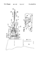
- FIG. 1 is a plan view of a first embodiment of the end effector of this invention shown inserted into a semiconductor wafer cassette to retrieve or replace a wafer.
- FIG. 2 is a side elevation view of the end effector of FIG. 1 without the wafer cassette but showing the end effector inserted between an adjacent pair of three closely spaced apart wafers as they would be stored in the cassette.
- FIG. 3 is an enlarged side elevation view of a flat rest pad embodiment of this invention showing the rest pad engaging an exclusion zone of a wafer.
- FIG. 4 is an enlarged side elevation view of an inclined rest pad embodiment of this invention showing the inclined rest pad engaging substantially a periphery of a wafer.
- FIG. 5 is a fragmentary plan view of a portion of the end effector and wafer of FIG. 1, enlarged to reveal positional relationships among the wafer and a movable contact point, wafer rest pads, and wafer edge and elevation sensors of the first embodiment end effector of this invention.
- FIGS. 6A and 6B are respective side and front elevation views of one of the edge and elevation sensors of FIG. 5, further enlarged to reveal the positioning of fiber optic light paths relative to the wafer.
- FIG. 7 is a plan view of a second embodiment of the end effector of this invention shown gripping a semiconductor wafer and adjacent to a semiconductor wafer in a wafer cassette to sense, retrieve, or replace a wafer.
- FIG. 8 is a sectional side elevation view of the end effector of FIG. 7 showing a preferred active contact point actuating mechanism gripping a wafer between adjacent ones of closely spaced apart wafers as they would be stored in the wafer cassette.
- FIG. 9 is an enlarged isometric view of a distal arcuate rest pad embodiment of this invention mounted on the distal end of the end effector of FIG. 7 .
- FIG. 10 is an end perspective view of the end effector of FIG. 7 showing positional relationships among the movable contact point, arcuate rest pads, and wafer edge and elevation sensors of the second embodiment end effector of this invention.
- FIG. 11 is a bottom view of the end effector of FIG. 7 showing fiber optic routing channels for elevation sensors of the second embodiment end effector of this invention.
- FIGS. 1 and 2 show a first embodiment of a spatula-shaped end effector 10 of this invention for transferring semiconductor wafers, such as a wafer 12 (shown transparent to reveal underlying structures), to and from a wafer cassette 14 .
- End effector 10 is adapted to receive and securely hold wafer 12 and transfer it to and from cassette 14 for processing.
- FIG. 2 shows that end effector 10 is particularly adapted for retrieving and replacing wafer 12 from among closely spaced apart wafers, such as wafers 12 , 12 A, and 12 B, which are shown as they might be stacked in wafer cassette 14 .
- Wafers having diameters of less than 150 mm are typically spaced apart at a 4.76 mm ( ⁇ fraction (3/16) ⁇ inch) pitch distance, 200 mm diameter wafers are typically spaced apart at a 6.35 mm ( ⁇ fraction (3/16) ⁇ inch) pitch distance, and 300 mm wafers are typically spaced apart at a 10 mm (0.394 inch) pitch distance.
- End effector 10 is operably attached to a robot arm 16 (a portion of which is shown) that is programmably positionable in a well known manner.
- end effector 10 enters wafer cassette 14 to retrieve wafer 12 positioned between wafers 12 A and 12 B.
- End effector 10 is then finely positioned by robot arm 16 and actuated to grip a periphery 18 of wafer 12 , remove wafer 12 from cassette 14 , and transfer wafer 12 to a processing station (not shown) for processing.
- End effector 10 may then, if necessary, reinsert wafer 12 into cassette 14 , release wafer 12 , and withdraw from cassette 14 .
- End effector 10 is operably coupled to robot arm 16 at a proximal end 20 and extends to a distal end 22 .
- End effector 10 receives wafer 12 between proximal end 20 and distal end 22 and includes at least two and, preferably, four rest pads upon which wafer 12 is initially loaded.
- Two distal rest pads 24 are located at, or adjacent to, distal end 22 of end effector 10 , and at least one, but preferably two proximal rest pads 26 are located toward proximal end 20 .
- Distal rest pads 24 may alternatively be formed as a single arcuate rest pad having an angular extent greater than the length of a “flat,” which is a grain orientation indicating feature commonly found on semiconductor wafers.
- a flat 27 is shown, by way of example only, positioned between proximal rest pads 26 .
- wafer 12 may have a different orientation, so periphery 18 is also shown positioned between proximal rest pads 26 .
- Wafer 12 includes an exclusion zone 30 (a portion of which is shown in dashed lines).
- Semiconductor wafers have an annular exclusion zone, or inactive portion, that extends inwardly about 1 mm to about 5 mm from periphery 18 and completely surrounding wafer 12 .
- Exclusion zone 30 is described as part of an industry standard wafer edge profile template in SEMI (Semiconductor Equipment and Materials International) specification M10298, pages 18 and 19. As a general rule, no part of end effector 10 may contact wafer 12 beyond the inner boundary of exclusion zone 30 . It is anticipated that future versions of the specification may allow edge contact only, a requirement that is readily accommodated by this invention.
- Rest pads 24 and 26 each have an angular extent greater than any feature on wafer 12 to guarantee that wafer 12 is gripped only within exclusion zone 30 .
- Rest pads 24 and 26 may be made of various materials, but a preferred material is polyetheretherkeytone (“peek”), which is a semi-crystalline high temperature thermoplastic manufactured by Ensinger Engineering Plastics located in Washington, Pennsylvania. The rest pad material may be changed to adapt to different working environments, such as in high temperature applications.
- FIG. 3 shows a substantially flat embodiment of distal rest pads 24 that is suitable for use with wafers having less than about a 200 mm diameter.
- Distal rest pads 24 include a pad portion 32 and a backstop portion 34 .
- pad portion 32 is substantially parallel to an imaginary plane 36 extending through wafer 12
- backstop portion 36 is inclined toward wafer 12 at a backstop angle 38 of up to about 5 degrees relative to a line perpendicular to plane 36 .
- pad portion 32 may be inclined away from wafer 12 up to about 3 degrees relative to plane 36 .
- Pad portion 32 has a length 40 that is a function of the depth of exclusion zone 30 , but is preferably about 3 mm long.
- Wafer 12 typically has a substantially rounded peripheral edge and contacts rest pads 24 only within exclusion zone 30 . Wafer 12 is gripped by urging it into the included angle formed between pad portion 32 and backstop portion 34 .
- FIG. 4 shows an inclined embodiment of distal rest pads 24 that is suitable for use with wafers having greater than about a 200 mm diameter, and preferably about a 300 mm or larger diameter. Of course, this invention may also be used for smaller diameter wafers.
- Distal rest pads 24 include an inclined pad portion 42 and a backstop portion 34 .
- inclined pad portion 42 is inclined away from wafer 12 at a rest pad angle 44 of about 3 degrees relative to plane 36
- backstop portion 36 is inclined toward wafer 12 at backstop angle 38 of up to about 3 degrees.
- Inclined pad portion 42 has a length 40 that is a function of the depth of exclusion zone 30 , but is preferably about 3 mm long.
- wafer 12 typically has a substantially rounded peripheral edge and contacts rest pads 24 only within exclusion zone 30 .
- Wafer 12 is gripped by urging it into the included angle formed between pad portion 42 and backstop portion 34 .
- This rest pad embodiment is also suitable for wafer edge contact only.
- Both the flat and inclined embodiments of distal rest pads 24 have a height 48 that substantially reaches but does not extend beyond the top surface of wafer 12 .
- proximal rest pads 26 are similar to distal rest pads 24 except that each rest pad 26 does not necessarily require a backstop portion and its pad portion has a length of about twice that of length 40 .
- End effector 10 further includes an active contact point 50 that is located at proximal end 20 of end effector 10 and between proximal rest pads 26 .
- Active contact point 50 is movable between a retracted wafer-loading position (shown in dashed lines) and an extended wafer-gripping position (shown in solid lines).
- Active contact point 50 is operatively connected to a piston 52 for reciprocation between the retracted and extended positions.
- piston 52 reciprocates within a bore 54 and is preferably vacuum pressure operated to extend and retract active contact point 50 .
- Active contact point 50 is connected to piston 52 by a piston rod 56 that extends through an airtight seal 58 .
- Bore 54 forms a vacuum chamber in end effector 10 that is divided by piston 52 into a drive chamber 60 and a return chamber 62 .
- Drive chamber 60 is in pneumatic communication with a vacuum pressure source (not shown) through a first channel 64
- return chamber 62 is in pneumatic communication with the vacuum pressure source through a second channel 66 .
- the vacuum pressure acts through drive chamber 60 against the front face of piston 52 to extend active contact point 50 to the wafer-gripping position and acts through return chamber 62 against the back face of piston 52 to retract active contact point 50 as controlled by the programmable control.
- the vacuum pressure source is routed to first and second channels 64 and 66 through rotary vacuum communication spools in robot arm 16 .
- Preferred rotary vacuum communication spools are described in U.S. Pat. No. 5,741,113 for CONTINUOUSLY ROTATABLE MULTIPLE LINK ROBOT ARM MECHANISM, which is assigned to the assignee of this application.
- Piston 52 further includes an annular groove 68 that is in pneumatic communication with a vent (not shown) in piston rod 56 .
- First and second channels 64 and 66 are connected respectively to drive chamber 60 and return chamber 62 at locations that are opened to groove 68 at the travel limits of piston 52 . Therefore, vacuum pressure in first and second channels 64 and 66 is reduced at the travel limits of piston 52 , thereby providing signals to the vacuum controller that active contact point 50 is fully extended or retracted to effect proper loading of wafer 12 .
- active contact point 50 is actuated to move wafer 12 into its gripped position. As active contact point 50 is extended, it urges wafer 12 toward distal rest pads 24 until wafer 12 is gripped within exclusion zone 30 by active contact point 50 and distal rest pads 24 .
- Proximal rest pads 26 are arranged relative to distal rest pads 24 so that plane 36 of wafer 12 is preferably parallel to end effector 10 when gripped. This arrangement is readily achieved when the flat embodiment of proximal and distal rest pads 24 and 26 is employed. However, when the inclined embodiment is employed, proximal and distal rest pads 24 and 26 are arranged such that the points where wafer 12 contacts pad portions 42 are substantially equidistant from a center 70 of wafer 12 when active contact point 50 is extended and wafer 12 is gripped. For example, when wafer 12 is in the position shown in FIG. 1, the pad portions of distal and proximal rest pads 24 and 26 contact wafer 12 at points tangent to periphery 18 such that a line through the center of each pad portion 42 intersects center 70 of wafer 12 .
- active contact point 50 at proximal end 20 allows end effector 10 to be lighter, stronger, and more slender than end effectors having moving mechanisms that may not fit between adjacent wafers 12 , 12 A, and 12 B in cassette 14 .
- the lack of moving mechanisms further causes end effector 10 to produce less contamination within cassette 14 .
- locating active contact point 50 at proximal end 20 of end effector 10 ensures that active contact point 50 is remote from harsh conditions such as heated environments and liquids.
- FIGS. 5, 6 A, and 6 B show respective top, side, and front views of a first embodiment of wafer edge and elevation sensors that provide accurate wafer 12 positioning data relative to end effector 10 .
- Wafer 12 is shown transparent to reveal underlying structures.
- the sensors are housed in first and second sensor housings 80 and 82 , which together form three light transmission sensors, each having a fiber optic source/receiver pair.
- First and second sensor housings 80 and 82 each include a light source fiber 84 and a light receiver fiber 86 that form between them a small U-shaped opening 88 into which periphery 18 of wafer 12 can fit. Fibers 84 and 86 further include mutually facing light path openings 90 that form a narrow light transmission pathway for detecting the presence or absence of periphery 18 of wafer 12 . Fibers 84 and 86 extend through ferrules 92 to a light source/receiver module 94 that is mounted on a convenient location of end effector 10 near its rotary connection to robot arm 16 .
- Light source/receiver module 94 conventionally detects degrees of light transmission between fibers 84 and 86 and, thereby, accurately senses the positioning of periphery 18 between light path openings 90 .
- the relative positions of fibers 84 and 86 may be reversed.
- First sensor housing 80 further includes a light source fiber 96 (shown in phantom), and second sensor housing 82 includes a light receiver fiber 98 (shown in phantom). Fibers 96 and 98 form between them a wide opening that sights along a bottom surface chord 100 of wafer 12 . Fibers 96 and 98 further include mutually facing light path openings 102 that form a narrow light transmission pathway 104 for detecting the presence or absence of bottom surface chord 100 of wafer 12 . Fibers 96 and 98 extend through ferrules 106 to light source/receiver module 94 .
- Light source/receiver module 94 conventionally detects degrees of light transmission between fibers 96 and 98 and thereby accurately senses the positioning of bottom surface chord 100 between light path openings 102 .
- the relative positions of fibers 96 and 98 may be reversed.
- Flat 27 may be detected by separating light path openings 102 from each other by distance greater than the length of flat 27 .
- Flat 27 is present if bottom surface chord 100 is sensed between light path openings 102 , but periphery 18 is not sensed between one of the pairs of light path openings 90 .
- end effector 10 accesses wafer 12 of a known diameter, such as 200 mm, is described below with reference to FIGS. 2, 5 , 6 A, and 6 B.
- Active contact point 50 is placed in its retracted position.
- End effector 10 is inserted in an X direction into cassette 14 between, for example, wafers 12 and 12 B, until periphery 18 is sensed between at least one pair of light path openings 90 .
- a controller (not shown) associated with robot arm 16 records the extension of robot arm 16 when periphery 18 is sensed, ignoring any sensed flat.
- End effector 10 is retracted in the ⁇ X direction by an amount sufficient to provide clearance between wafer 12 and the edge detectors.
- Robot arm 16 is moved in a Z direction until bottom surface chord 100 of wafer 12 is sensed.
- the controller records the Z elevation of the bottom surface of wafer 12 .
- the controller computes the X distance required to reach into cassette 14 at a Z elevation below the bottom surface of wafer 12 so distal and proximal rest pads 24 and 26 clear wafers 12 and 12 B.
- the controller also accounts for:
- the controller moves end effector 10 in the X direction into cassette 14 and elevates in the Z direction to contact wafer 12 on landing pads 24 and 26 .
- Active contact point 50 is actuated to urge wafer 12 into the included angle between pad and backstop portions 32 and 34 of distal rest pads 24 , thereby gripping wafer 12 .
- End effector 10 withdraws wafer 12 in the ⁇ X direction from cassette 14 .
- FIGS. 7 and 8 show a second embodiment of a spatula-shaped end effector 110 of this invention for transferring semiconductor wafers, such as wafer 12 (shown transparent to reveal underlying structures), to and from wafer cassette 14 (not shown in this view).
- End effector 110 is similar to end effector 10 but is further adapted to sense the bottom surface of a wafer stored in wafer cassette 14 without protruding into the cassette.
- FIG. 8 shows that end effector 110 is particularly adapted for retrieving and replacing wafer 12 from among closely spaced apart wafers, such as wafers 12 , 12 A, and 12 B, which are shown as they might be stacked in wafer cassette 14 .
- End effector 110 is operably attached to robot arm 16 .
- end effector 110 senses the bottom surface of wafer 12 before entering wafer cassette 14 to retrieve wafer 12 from between wafers 12 A and 12 B.
- End effector 110 is then finely positioned by robot arm 16 and actuated to grip periphery 18 of wafer 12 , remove wafer 12 from cassette 14 , and transfer wafer 12 to a processing station (not shown) for processing.
- End effector 110 may then, if necessary, reinsert wafer 12 into cassette 14 , release wafer 12 , and withdraw from cassette 14 .
- End effector 110 is operably coupled to robot arm 16 at a proximal end 120 and extends to a distal end 122 .
- End effector 110 receives wafer 12 between proximal end 120 and distal end 122 and includes at least two and, preferably, four arcuate rest pads upon which wafer 12 is initially loaded.
- Two distal arcuate rest pads 124 are located at, or adjacent to, distal end 122 of end effector 110 ; and at least one, but preferably two proximal arcuate rest pads 126 are located toward proximal end 120 .
- Distal and proximal arcuate rest pads 124 and 126 may have an angular extent greater than flat 27 , which is shown, by way of example only, positioned between proximal rest pads 126 .
- wafer 12 may have a different orientation from that shown.
- Arcuate rest pads 124 and 126 whether separated as shown, or joined into a single rest pad, have an angular extent greater than any feature on wafer 12 to guarantee that wafer 12 is sufficiently gripped, whether flatted or not, and only within exclusion zone 30 .
- rest pads 124 and 126 may be made of various materials, but the preferred material is peek.
- FIG. 9 shows the embodiment of distal arcuate rest pads 124 that is suitable for use with flatted or nonflatted wafers having greater than about a 200 mm diameter, and preferably a 300 mm or larger diameter. Of course, this invention may also be used for smaller or larger diameter wafers.
- Distal arcuate rest pads 124 include an inclined pad portion 132 and a backstop portion 134 . Referring also to FIG. 4, inclined pad portion 132 is inclined away from wafer 12 at rest pad angle 44 of about 3 degrees relative to plane 36 , and backstop portion 136 is inclined toward wafer 12 at backstop angle 38 of up to about 3 degrees.
- Inclined pad portion 132 has a length 140 that is a function of the depth of exclusion zone 30 , but is preferably about 3 mm long.
- wafer 12 typically has a substantially rounded peripheral edge and contacts arcuate rest pads 124 only within exclusion zone 30 . Of course, the peripheral edge need not be rounded. Wafer 12 is gripped by urging it into the included angle formed between inclined pad portion 132 and backstop portion 134 . This arcuate rest pad embodiment is also suitable for wafer edge contact only.
- Distal arcuate rest pads 124 have a height 148 that substantially reaches but does not extend beyond the top surface of wafer 12 .
- proximal arcuate rest pads 126 are similar to distal arcuate rest pads 124 except that each rest pad 126 does not necessarily require a backstop portion and its pad portion has a length of about twice that of length 140 .
- End effector 110 further includes an active contact point 150 that is located at proximal end 120 of end effector 110 and between proximal arcuate rest pads 126 .
- Active contact point 150 is movable between a retracted wafer-loading position (not shown) and the extended wafer-gripping position shown.
- Active contact point 150 is operatively connected to a piston 152 for reciprocation between retracted and extended positions.
- piston 152 reciprocates within a bore 154 and is urged by a spring 155 to extend active contact point and by a vacuum pressure to retract active contact point 150 .
- Active contact point 150 is connected to piston 152 by a piston rod 156 that extends through an annular airtight seal 158 .
- Bore 154 includes an end cap 159 that forms one wall of a vacuum chamber 160 , the other wall of which is movably formed by piston 152 .
- Vacuum chamber 160 is in pneumatic communication with a vacuum pressure source (not shown) through a vacuum feedthrough 162 and a vacuum channel 164 .
- Spring 155 presses against the face of piston 152 to extend active contact point 150 to the wafer-gripping position, whereas the vacuum pressure acts through vacuum chamber 160 against the face of piston 152 to overcome the spring force and retract active contact point 150 to the wafer-releasing position.
- active contact point 150 is urged against wafer 12 with a force determined solely by spring 155 .
- Spring 155 is supported between recesses 166 in piston 152 and end cap 159 .
- the vacuum pressure source is routed to vacuum channel 164 through rotary vacuum communication seals or spools in robot arm 16 .
- Actuating mechanism 151 further includes a vent 168 in pneumatic communication with the atmosphere to allow free movement of piston 152 within the portion of bore 154 not in pneumatic communication with the vacuum pressure source.
- Actuating mechanism is made “vacuum tight” by O-ring seals 170 surrounding end cap 159 and vacuum feedthrough 162 and by an annular moving seal 172 surrounding piston 152 .
- 0 -ring bumper seals 174 fitted to the faces of piston 152 absorb contact shocks potentially encountered by piston 152 at the extreme ends of its travel.
- active contact point 150 is actuated to move wafer 12 into its gripped position. As active contact point 150 is extended by spring 155 , it urges wafer 12 toward distal arcuate rest pads 124 until wafer 12 is gripped within exclusion zone 30 by active contact point 150 and distal arcuate rest pads 124 . Active contact point 150 includes an inwardly inclined face portion 176 that urges wafer 12 toward proximal arcuate rest pads 126 , thereby firmly gripping exclusion zone 30 of wafer 12 .
- Proximal arcuate rest pads 126 are arranged relative to distal arcuate rest pads 124 so that the plane of wafer 12 is preferably parallel to end effector 110 when gripped.
- end effector 110 In a manner similar to end effector 10 , the location of active contact point 150 at proximal end 120 allows end effector 110 to be lighter, stronger, and more slender than end effectors having moving mechanisms that may not fit between adjacent wafers 12 , 12 A, and 12 B in cassette 14 . The lack of moving mechanisms between its proximal and distal ends further causes end effector 110 to produce less contamination within cassette 14 . Moreover, unlike end effector 10 , which is actuated by two vacuum lines, end effector 100 requires only one vacuum line for actuation. Of course, end effector 10 could be fitted with actuating mechanism 151 .
- FIGS. 7, 10 , and 11 show respective top, end, and bottom views of a second embodiment of wafer edge and elevation sensors that provide accurate wafer 12 positioning data relative to end effector 110 .
- the wafer edge sensors are housed in first and second sensor housings 180 and 182 , each having a fiber optic source/receiver pair forming a light transmission sensor in each housing.
- the elevation sensor is housed in distal end 122 of end effector 110 .
- First and second sensor housings 180 and 182 each include light source fiber 84 and light receiver fiber 86 , as in end effector 10 , that form between them a small U-shaped opening 88 into which periphery 18 of wafer 12 can fit.
- fibers 84 and 86 include mutually facing light path openings that form a narrow light transmission pathway for detecting the presence or absence of periphery 18 of wafer 12 .
- the two wafer edge sensors are separated from each other by a distance 183 greater than the length of flat 27 so that a flatted wafer can be detected when only one of the two wafer edge sensors detects periphery 18 of wafer 12 .
- wafer 12 must be appropriately oriented in cassette 14 to detect flat 27 .
- first and second sensor housings 180 and 182 do not include light source fiber 96 light receiver fiber 98 .
- light source fiber 96 is routed through a first channel 184 formed in the bottom surface of end effector 110 and running between proximal end 120 and a first distal tine 188 proximal to distal end 122 of end effector 110 .
- light receiver fiber 98 is routed through a second channel 186 formed in the bottom surface of end effector 110 and running between proximal end 120 and a second distal tine 190 proximal to distal end 122 of end effector 110 .
- Distal tines 188 and 190 are widely spaced apart across a gap 191 that forms a relief region for certain types of processing equipment, such as wafer prealigners.
- Fibers 96 and 98 terminate in mutually facing light path openings 192 and 194 formed in distal tines 188 and 190 . Fibers 96 and 98 form between them a wide opening that sights along a bottom surface chord 200 of, for example, wafer 12 A.
- Mutually facing light path openings 192 and 194 form a narrow light transmission pathway 202 for detecting the presence or absence of bottom surface chord 200 of wafer 12 A.
- light transmission pathway 202 extends beyond the portion of distal end 122 that would first contact wafer 12 , thereby further providing an obstruction sensing capability.
- light source/receiver module 94 conventionally detects degrees of light transmission between fibers 96 and 98 and, thereby, accurately senses the positioning of bottom surface chord 200 between light path openings 192 and 194 .
- the relative positions of fibers 96 and 98 may be reversed.
- end effector 110 accesses a predetermined wafer from among closely spaced apart wafers in a cassette, is described below with reference to FIGS. 7, 8 , and 10 .
- Active contact point 150 is placed in its retracted position.
- End effector 110 is moved in an X direction toward cassette 14 until tines 188 and 190 are adjacent to, but not touching, a predicted position for any wafer 12 in cassette 14 .
- End effector 110 is then scanned in a Z direction such that light transmission pathway 202 intersects the bottom surface chord 200 of any wafer in cassette 14 and, additionally, detects any obstruction projecting from cassette 14 toward end effector 110 .
- the controller (not shown) records the Z elevations of the bottom surfaces of any wafers and obstructions detected.
- Robot arm 16 is moved to a Z elevation calculated to access a predetermined wafer, such as wafer 12 A, while also providing clearance for end effector 110 between adjacent wafers.
- End effector 110 may be optionally moved in an X direction toward cassette 14 until tines 188 and 190 are adjacent to, but not touching, wafer 12 A. In this position, light transmission pathway 202 should be adjacent to bottom surface chord 200 of wafer 12 A;
- robot arm 16 is optionally moved in a Z direction until bottom surface chord 200 of wafer 12 A is sensed;
- the controller optionally verifies the previously sensed Z elevation of the bottom surface of wafer 12 A;
- robot arm 16 is optionally moved in a ⁇ Z direction to provide clearance for end effector 110 between adjacent wafers.
- End effector 110 is inserted in an X direction into cassette 14 between adjacent wafers until periphery 18 is sensed between at least one wafer edge sensor.
- the controller moves end effector 10 in the Z direction calculated to contact wafer 12 A on landing pads 124 and 126 .
- Active contact point 150 is actuated to urge wafer 12 A into the included angle between pad and backstop portions 132 and 134 of distal arcuate rest pads 124 , thereby gripping wafer 12 A. (In FIG. 7, the gripped wafer is shown as wafer 12 .)
- End effector 110 withdraws wafer 12 A in the ⁇ X direction from cassette 14 .
- End effector 110 combines a very thin Z-direction profile and accurate wafer position sensing to enable clean, rapid, and secure movement of very closely spaced apart wafers in a cassette.
- the pistons may be actuated by alternative power sources, such as, for example, by a pulsing solenoid that slows the pistons as wafer 12 is secured. Electric signals may be employed to drive and monitor the positioning of the pistons.
- the pistons may also be pneumatically operated and monitored, such as in applications where the end effectors are submerged in a liquid.
- the end effectors may be forked or otherwise include a cutout or be shaped to avoid obstacles, such as a prealigner hub.
- the end effector is usable for handling various types of specimens other than semiconductor wafers, such as compact diskettes and computer memory discs.
Abstract
Description
Claims (19)
Priority Applications (21)
| Application Number | Priority Date | Filing Date | Title |
|---|---|---|---|
| US09/204,747 US6256555B1 (en) | 1998-12-02 | 1998-12-02 | Robot arm with specimen edge gripping end effector |
| US09/312,343 US6275748B1 (en) | 1998-12-02 | 1999-05-14 | Robot arm with specimen sensing and edge gripping end effector |
| PCT/US1999/028737 WO2000033359A2 (en) | 1998-12-02 | 1999-12-02 | Specimen holding robotic arm end effector |
| IL14346799A IL143467A (en) | 1998-12-02 | 1999-12-02 | Specimen holding robotic arm and effector |
| US09/890,839 US6453214B1 (en) | 1998-12-02 | 1999-12-02 | Method of using a specimen sensing end effector to align a robot arm with a specimen stored on or in a container |
| DE69938360T DE69938360T2 (en) | 1998-12-02 | 1999-12-02 | PULSE GRIP FOR PROBE HALTEROBOTER |
| EP99964097A EP1135795B1 (en) | 1998-12-02 | 1999-12-02 | Specimen holding robotic arm end effector |
| AU20410/00A AU2041000A (en) | 1998-12-02 | 1999-12-02 | Specimen holding robotic arm end effector |
| KR1020017006882A KR100749905B1 (en) | 1998-12-02 | 1999-12-02 | Specimen holding robotic arm end effector, and method of using as such, and edge-gripping device |
| AT99964097T ATE389237T1 (en) | 1998-12-02 | 1999-12-02 | ARM GRIP FOR SAMPLE HOLDER ROBOTS |
| CNB998140325A CN1238882C (en) | 1998-12-02 | 1999-12-02 | Specimen holding robotic arm end effector |
| JP2000585915A JP2002531942A (en) | 1998-12-02 | 1999-12-02 | Robot arm end effector holding sample |
| CNB2005101376380A CN100373580C (en) | 1998-12-02 | 1999-12-02 | Robot arm with specimen edge gripping end effector |
| US09/920,353 US6438460B1 (en) | 1998-12-02 | 2001-08-01 | Method of using a specimen sensing end effector to determine the thickness of a specimen |
| HK02102462.3A HK1041104B (en) | 1998-12-02 | 2002-04-03 | Specimen holding robotic arm end effector |
| US10/223,075 US6618645B2 (en) | 1998-12-02 | 2002-08-15 | Method of using a specimen sensing end effector to determine angular orientation of a specimen |
| US10/649,116 US6898487B2 (en) | 1998-12-02 | 2003-08-26 | Specimen sensing and edge gripping end effector |
| IL166019A IL166019A (en) | 1998-12-02 | 2004-12-21 | Method of removing a specimen from a specimen holder |
| IL166018A IL166018A (en) | 1998-12-02 | 2004-12-28 | Specimen peripheral edge-gripping device that is adapted for operative coupling to a mechanism and gripping a specimen |
| US11/136,078 US7233842B2 (en) | 1998-12-02 | 2005-05-23 | Method of determining axial alignment of the centroid of an edge gripping end effector and the center of a specimen gripped by it |
| JP2010006284A JP5518497B2 (en) | 1998-12-02 | 2010-01-14 | Method for determining alignment between an end effector and a sample having a peripheral edge, and an apparatus for transferring a sample comprising the end effector |
Applications Claiming Priority (1)
| Application Number | Priority Date | Filing Date | Title |
|---|---|---|---|
| US09/204,747 US6256555B1 (en) | 1998-12-02 | 1998-12-02 | Robot arm with specimen edge gripping end effector |
Related Child Applications (1)
| Application Number | Title | Priority Date | Filing Date |
|---|---|---|---|
| US09/312,343 Continuation-In-Part US6275748B1 (en) | 1998-12-02 | 1999-05-14 | Robot arm with specimen sensing and edge gripping end effector |
Publications (1)
| Publication Number | Publication Date |
|---|---|
| US6256555B1 true US6256555B1 (en) | 2001-07-03 |
Family
ID=22759269
Family Applications (2)
| Application Number | Title | Priority Date | Filing Date |
|---|---|---|---|
| US09/204,747 Expired - Lifetime US6256555B1 (en) | 1998-12-02 | 1998-12-02 | Robot arm with specimen edge gripping end effector |
| US09/312,343 Expired - Lifetime US6275748B1 (en) | 1998-12-02 | 1999-05-14 | Robot arm with specimen sensing and edge gripping end effector |
Family Applications After (1)
| Application Number | Title | Priority Date | Filing Date |
|---|---|---|---|
| US09/312,343 Expired - Lifetime US6275748B1 (en) | 1998-12-02 | 1999-05-14 | Robot arm with specimen sensing and edge gripping end effector |
Country Status (5)
| Country | Link |
|---|---|
| US (2) | US6256555B1 (en) |
| JP (1) | JP5518497B2 (en) |
| KR (1) | KR100749905B1 (en) |
| CN (1) | CN100373580C (en) |
| DE (1) | DE69938360T2 (en) |
Cited By (108)
| Publication number | Priority date | Publication date | Assignee | Title |
|---|---|---|---|---|
| WO2001083171A1 (en) * | 2000-05-03 | 2001-11-08 | Berkeley Process Control, Inc. | Self teaching robotic wafer handling system |
| US6322312B1 (en) | 1999-03-18 | 2001-11-27 | Applied Materials, Inc. | Mechanical gripper for wafer handling robots |
| US6453214B1 (en) * | 1998-12-02 | 2002-09-17 | Newport Corporation | Method of using a specimen sensing end effector to align a robot arm with a specimen stored on or in a container |
| US6454332B1 (en) * | 1998-12-04 | 2002-09-24 | Applied Materials, Inc. | Apparatus and methods for handling a substrate |
| US6468022B1 (en) | 2000-07-05 | 2002-10-22 | Integrated Dynamics Engineering, Inc. | Edge-gripping pre-aligner |
| US6502054B1 (en) | 1999-11-22 | 2002-12-31 | Lam Research Corporation | Method of and apparatus for dynamic alignment of substrates |
| US6513848B1 (en) | 1999-09-17 | 2003-02-04 | Applied Materials, Inc. | Hydraulically actuated wafer clamp |
| US6528767B2 (en) | 2001-05-22 | 2003-03-04 | Applied Materials, Inc. | Pre-heating and load lock pedestal material for high temperature CVD liquid crystal and flat panel display applications |
| US20030082042A1 (en) * | 2001-07-13 | 2003-05-01 | Woodruff Daniel J. | End-effectors for handling microelectronic workpieces |
| US20030085582A1 (en) * | 2001-07-13 | 2003-05-08 | Woodruff Daniel J. | End-effectors for handling microelectronic workpieces |
| US20030098047A1 (en) * | 2001-11-13 | 2003-05-29 | Herbst Tim W. | Semiconductor wafer cleaning systems and methods |
| US20030130759A1 (en) * | 2001-09-04 | 2003-07-10 | Boris Kesil | Precision soft-touch gripping mechanism for flat objects |
| US20030151268A1 (en) * | 1998-07-10 | 2003-08-14 | Holbrooks Orville Ray | Intelligent integrated circuit wafer handling system with fail safe system |
| US6629053B1 (en) * | 1999-11-22 | 2003-09-30 | Lam Research Corporation | Method and apparatus for determining substrate offset using optimization techniques |
| US6634686B2 (en) | 2001-10-03 | 2003-10-21 | Applied Materials, Inc. | End effector assembly |
| US6652216B1 (en) | 1998-05-05 | 2003-11-25 | Recif, S.A. | Method and device for changing a semiconductor wafer position |
| US20030219914A1 (en) * | 2002-01-29 | 2003-11-27 | Recif, S. A. | Apparatus and process for identification of characters inscribed on a semiconductor wafer containing an orientation mark |
| US6678581B2 (en) * | 2002-01-14 | 2004-01-13 | Taiwan Semiconductor Manufacturing Co. Ltd | Method of calibrating a wafer edge gripping end effector |
| US20040013503A1 (en) * | 2002-07-22 | 2004-01-22 | Jaswant Sandhu | Robotic hand with multi-wafer end effector |
| US20040012363A1 (en) * | 2002-03-20 | 2004-01-22 | Fsi International, Inc. | Systems and methods incorporating an end effector with a rotatable and/or pivotable body and/or an optical sensor having a light path that extends along a length of the end effector |
| US20040012214A1 (en) * | 2000-08-04 | 2004-01-22 | Casarotti Sean A. | Detection and handling of semiconductor wafers and wafers-like objects |
| US20040048474A1 (en) * | 2000-12-15 | 2004-03-11 | Hiroshi Asano | Wafer holding |
| US20040050405A1 (en) * | 2002-09-13 | 2004-03-18 | Christenson Kurt K. | Semiconductor wafer cleaning systems and methods |
| US20040067128A1 (en) * | 2002-10-08 | 2004-04-08 | Caveney Robert T. | Apparatus for alignment and orientation of a wafer for processing |
| US20040068347A1 (en) * | 2002-10-08 | 2004-04-08 | Martin Aalund | Substrate handling system for aligning and orienting substrates during a transfer operation |
| US20040102059A1 (en) * | 2002-11-25 | 2004-05-27 | John Dickinson | Atmospheric robot handling equipment |
| US20040102858A1 (en) * | 2001-09-04 | 2004-05-27 | Boris Kesil | Soft-touch gripping mechanism for flat objects |
| US20040113444A1 (en) * | 2002-12-17 | 2004-06-17 | Blonigan Wendell T. | End effector assembly |
| US6765223B2 (en) * | 2001-08-22 | 2004-07-20 | Agilent Technologies, Inc. | Sub-micron accuracy edge detector |
| US20040170407A1 (en) * | 2003-02-27 | 2004-09-02 | Applied Materials, Inc. | Substrate support |
| US20040226513A1 (en) * | 2003-05-12 | 2004-11-18 | Applied Materials, Inc. | Chamber for uniform heating of large area substrates |
| US20050017529A1 (en) * | 2003-07-21 | 2005-01-27 | Rogers Theodore W. | Active edge gripping end effector |
| US20050052041A1 (en) * | 2003-07-11 | 2005-03-10 | Bonora Anthony C. | Ultra low contact area end effector |
| US20050102064A1 (en) * | 2003-11-10 | 2005-05-12 | Applied Materials, Inc. | Method and apparatus for self-calibration of a substrate handling robot |
| US20050107917A1 (en) * | 2003-11-14 | 2005-05-19 | Smith Paul E. | Robotic system for sequencing multiple specimens between a holding tray and a microscope |
| US20050110287A1 (en) * | 2003-10-24 | 2005-05-26 | Ade Corporation | 200 MM notched/flatted wafer edge gripping end effector |
| US20050180737A1 (en) * | 2004-02-12 | 2005-08-18 | Applied Materials, Inc. | Substrate support bushing |
| US20050210669A1 (en) * | 2004-03-29 | 2005-09-29 | Kawasaki Jukogyo Kabushiki Kaisha | Substrate gripping apparatus, substrate gripping method and substrate releasing method |
| US20050229426A1 (en) * | 2001-11-02 | 2005-10-20 | Applied Materials, Inc. | Single wafer dryer and drying methods |
| US20050255244A1 (en) * | 2002-11-18 | 2005-11-17 | Applied Materials, Inc. | Lifting glass substrate without center lift pins |
| US20050265814A1 (en) * | 2003-09-10 | 2005-12-01 | Coady Matthew W | Substrate handling system for aligning and orienting substrates during a transfer operation |
| US20060005770A1 (en) * | 2004-07-09 | 2006-01-12 | Robin Tiner | Independently moving substrate supports |
| US20060043750A1 (en) * | 2004-07-09 | 2006-03-02 | Paul Wirth | End-effectors for handling microfeature workpieces |
| US20060051184A1 (en) * | 2004-09-04 | 2006-03-09 | Elliott Martin R | Methods and apparatus for mapping carrier contents |
| US20060131903A1 (en) * | 2004-12-16 | 2006-06-22 | Asyst Technologies, Inc. | Active edge grip rest pad |
| US20060157998A1 (en) * | 2005-01-18 | 2006-07-20 | Elik Gershenzon | Contamination-free edge gripping mechanism and method for loading/unloading and transferring flat objects |
| US20060174921A1 (en) * | 2001-11-02 | 2006-08-10 | Applied Materials, Inc. | Single wafer dryer and drying methods |
| US20060192400A1 (en) * | 2005-02-25 | 2006-08-31 | Woo-Young Kim | Wafer transfer apparatus |
| US20060222480A1 (en) * | 2005-03-30 | 2006-10-05 | Duhamel Michael A | Substrate transport apparatus with active edge gripper |
| US20060236941A1 (en) * | 2005-04-20 | 2006-10-26 | Applied Materials, Inc. | Passive wafer support for particle free wafer acceleration |
| US20070001638A1 (en) * | 2005-07-01 | 2007-01-04 | Fsi International, Inc. | Robot with vibration sensor device |
| US20070014656A1 (en) * | 2002-07-11 | 2007-01-18 | Harris Randy A | End-effectors and associated control and guidance systems and methods |
| US20070018469A1 (en) * | 2005-07-25 | 2007-01-25 | Multimetrixs, Llc | Contamination-free edge gripping mechanism with withdrawable pads and method for loading/unloading and transferring flat objects |
| US20070020080A1 (en) * | 2004-07-09 | 2007-01-25 | Paul Wirth | Transfer devices and methods for handling microfeature workpieces within an environment of a processing machine |
| US20070062454A1 (en) * | 2000-07-20 | 2007-03-22 | Applied Materials, Inc. | Method for dechucking a substrate |
| US20070137279A1 (en) * | 2005-12-20 | 2007-06-21 | Samsung Electronics Co., Ltd. | Transferring device |
| US20070147982A1 (en) * | 2005-12-22 | 2007-06-28 | Applied Materials, Inc. | Method of retaining a substrate during a substrate transferring process |
| US20070177963A1 (en) * | 2006-02-01 | 2007-08-02 | Tang Chee W | End effector for transferring a wafer |
| US20070176445A1 (en) * | 2006-02-01 | 2007-08-02 | Jin-Sung Kim | Apparatus and method for transferring wafers |
| US20070242381A1 (en) * | 2006-03-31 | 2007-10-18 | Kabushiki Kaisha Toshiba | Magnetic recording medium and magnetic recording/reproducing device |
| US20080147580A1 (en) * | 2003-11-10 | 2008-06-19 | Pannese Patrick D | Applications of neural networks |
| US20080155442A1 (en) * | 2003-11-10 | 2008-06-26 | Pannese Patrick D | Methods and systems for controlling a semiconductor fabrication process |
| US20080163094A1 (en) * | 2003-11-10 | 2008-07-03 | Pannese Patrick D | Methods and systems for controlling a semiconductor fabrication process |
| US20080166210A1 (en) * | 2007-01-05 | 2008-07-10 | Applied Materials, Inc. | Supinating cartesian robot blade |
| US20080213076A1 (en) * | 2007-03-02 | 2008-09-04 | Stephen Hanson | Edge grip end effector |
| US20080260500A1 (en) * | 2007-02-27 | 2008-10-23 | Meulen Peter Van Der | Batch substrate handling |
| US20090003979A1 (en) * | 2007-06-29 | 2009-01-01 | Varian Semiconductor Equipment Associates, Inc. | Techniques for handling substrates |
| US20090067956A1 (en) * | 2004-12-22 | 2009-03-12 | Tetsuya Ishikawa | Cluster tool architecture for processing a substrate |
| EP2033745A3 (en) * | 2007-06-05 | 2009-05-13 | Nidec Sankyo Corporation | Industrial robot |
| US20090175705A1 (en) * | 2006-05-09 | 2009-07-09 | Ken Nakao | Substrate transfer apparatus and vertical heat processing apparatus |
| US20090182454A1 (en) * | 2008-01-14 | 2009-07-16 | Bernardo Donoso | Method and apparatus for self-calibration of a substrate handling robot |
| US20090198377A1 (en) * | 2005-07-15 | 2009-08-06 | Kabushiki Kaisha Yaskawa Denki | Wafer position teaching method and teaching tool |
| US20090196718A1 (en) * | 2008-02-05 | 2009-08-06 | Inotera Memories, Inc. | Holding apparatus |
| US7651306B2 (en) | 2004-12-22 | 2010-01-26 | Applied Materials, Inc. | Cartesian robot cluster tool architecture |
| US7654596B2 (en) | 2003-06-27 | 2010-02-02 | Mattson Technology, Inc. | Endeffectors for handling semiconductor wafers |
| US7694688B2 (en) | 2007-01-05 | 2010-04-13 | Applied Materials, Inc. | Wet clean system design |
| US7718011B2 (en) | 1999-03-26 | 2010-05-18 | Applied Materials, Inc. | Apparatus for cleaning and drying substrates |
| US20100234992A1 (en) * | 2009-03-12 | 2010-09-16 | Taiwan Semiconductor Manufacturing Co., Ltd. | Semiconductor wafer robot alignment system and method |
| US20100258144A1 (en) * | 2009-04-14 | 2010-10-14 | International Test Solutions | Wafer manufacturing cleaning apparatus, process and method of use |
| US7819079B2 (en) | 2004-12-22 | 2010-10-26 | Applied Materials, Inc. | Cartesian cluster tool configuration for lithography type processes |
| US20110193361A1 (en) * | 2010-02-08 | 2011-08-11 | Chia-He Cheng | Robot arm plate |
| US20110241367A1 (en) * | 2010-02-26 | 2011-10-06 | Brooks Automation, Inc. | Robot edge contact gripper |
| US20120065779A1 (en) * | 2010-09-15 | 2012-03-15 | Seiko Epson Corporation | Robot |
| WO2012052865A2 (en) * | 2010-10-22 | 2012-04-26 | Lam Research Corporation | Dual sensing end effector with single sensor |
| US20130249225A1 (en) * | 2012-03-26 | 2013-09-26 | Disco Corporation | Robot hand |
| TWI423373B (en) * | 2007-10-19 | 2014-01-11 | Tokyo Electron Ltd | Workpiece transfer mechanism, workpiece transfer method and workpiece processing system |
| US20140086717A1 (en) * | 2012-09-25 | 2014-03-27 | Daihen Corporation | Workpiece conveying robot |
| US8911193B2 (en) | 2004-12-22 | 2014-12-16 | Applied Materials, Inc. | Substrate processing sequence in a cartesian robot cluster tool |
| US8942845B2 (en) | 2010-09-15 | 2015-01-27 | Seiko Epson Corporation | Robot |
| US20160008986A1 (en) * | 2014-07-08 | 2016-01-14 | Shenzhen China Star Optoelectronics Technology Co. Ltd. | Pick-and-place device for glass substrate |
| US9378997B2 (en) * | 2014-03-31 | 2016-06-28 | Ebara Corporation | Substrate holding mechanism, substrate transporting device, and semiconductor manufacturing apparatus |
| US9401296B2 (en) | 2011-11-29 | 2016-07-26 | Persimmon Technologies Corporation | Vacuum robot adapted to grip and transport a substrate and method thereof with passive bias |
| WO2017059194A1 (en) * | 2015-10-02 | 2017-04-06 | Verselus, Llc | System and method for autonomously teaching working points in a robotic disk test apparatus |
| US9618857B2 (en) | 2015-02-28 | 2017-04-11 | Kla-Tencor Corporation | End effectors and reticle handling at a high throughput |
| US9691651B2 (en) | 2005-01-28 | 2017-06-27 | Brooks Automation, Inc. | Substrate handling system for aligning and orienting substrates during a transfer operation |
| US9919430B1 (en) * | 2016-12-06 | 2018-03-20 | Jabil Inc. | Apparatus, system and method for providing an end effector |
| US9991152B2 (en) | 2014-03-06 | 2018-06-05 | Cascade Microtech, Inc. | Wafer-handling end effectors with wafer-contacting surfaces and sealing structures |
| US10002781B2 (en) | 2014-11-10 | 2018-06-19 | Brooks Automation, Inc. | Tool auto-teach method and apparatus |
| US10086511B2 (en) | 2003-11-10 | 2018-10-02 | Brooks Automation, Inc. | Semiconductor manufacturing systems |
| US10286549B2 (en) | 2015-12-16 | 2019-05-14 | Comau Llc | Adaptable end effector and method |
| US11020852B2 (en) | 2017-10-05 | 2021-06-01 | Brooks Automation, Inc. | Substrate transport apparatus with independent accessory feedthrough |
| US11155428B2 (en) | 2018-02-23 | 2021-10-26 | International Test Solutions, Llc | Material and hardware to automatically clean flexible electronic web rolls |
| US11211242B2 (en) | 2019-11-14 | 2021-12-28 | International Test Solutions, Llc | System and method for cleaning contact elements and support hardware using functionalized surface microfeatures |
| US11318550B2 (en) | 2019-11-14 | 2022-05-03 | International Test Solutions, Llc | System and method for cleaning wire bonding machines using functionalized surface microfeatures |
| EP4100994A4 (en) * | 2020-02-17 | 2023-03-15 | Jabil Inc. | Apparatus, system and method for providing a fiber optic coupler |
| US11673275B2 (en) | 2019-02-08 | 2023-06-13 | Yaskawa America, Inc. | Through-beam auto teaching |
| US11756811B2 (en) | 2019-07-02 | 2023-09-12 | International Test Solutions, Llc | Pick and place machine cleaning system and method |
| WO2023186508A1 (en) * | 2022-03-31 | 2023-10-05 | Asml Netherlands B.V. | End-effector and method for handling a substrate |
Families Citing this family (52)
| Publication number | Priority date | Publication date | Assignee | Title |
|---|---|---|---|---|
| KR20010032714A (en) * | 1997-12-03 | 2001-04-25 | 오노 시게오 | Substrate transferring device and method, exposure apparatus having the substrate transferring device, and method of manufacturing device using the exposure apparatus |
| SE513503C2 (en) * | 1998-08-26 | 2000-09-25 | Alfa Laval Agri Ab | Method and apparatus for controlling the movement of a robotic arm of a milking robot |
| AU742980B2 (en) * | 1999-10-13 | 2002-01-17 | Kawasaki Jukogyo Kabushiki Kaisha | Random work arranging device |
| DE10061628B4 (en) * | 2000-12-11 | 2006-06-08 | Leica Microsystems Wetzlar Gmbh | Apparatus and method for gripping and transporting wafers |
| US6879876B2 (en) * | 2001-06-13 | 2005-04-12 | Advanced Technology Materials, Inc. | Liquid handling system with electronic information storage |
| US6918731B2 (en) * | 2001-07-02 | 2005-07-19 | Brooks Automation, Incorporated | Fast swap dual substrate transport for load lock |
| US6643563B2 (en) * | 2001-07-13 | 2003-11-04 | Brooks Automation, Inc. | Trajectory planning and motion control strategies for a planar three-degree-of-freedom robotic arm |
| WO2003009346A2 (en) * | 2001-07-15 | 2003-01-30 | Applied Materials,Inc. | Processing system |
| US7371041B2 (en) * | 2001-08-30 | 2008-05-13 | Seagate Technology Llc | Assembly station with rotatable turret which forms and unloads a completed stack of articles |
| JP3795820B2 (en) * | 2002-03-27 | 2006-07-12 | 株式会社東芝 | Substrate alignment device |
| US6808589B2 (en) * | 2002-06-14 | 2004-10-26 | Taiwan Semiconductor Manufacturing Co. Ltd | Wafer transfer robot having wafer blades equipped with sensors |
| US6893070B2 (en) * | 2002-10-17 | 2005-05-17 | Delaware Capital Formation, Inc. | Integrated end effector |
| US20040112544A1 (en) * | 2002-12-16 | 2004-06-17 | Hongwen Yan | Magnetic mirror for preventing wafer edge damage during dry etching |
| US7107125B2 (en) * | 2003-10-29 | 2006-09-12 | Applied Materials, Inc. | Method and apparatus for monitoring the position of a semiconductor processing robot |
| US7181314B2 (en) * | 2003-11-24 | 2007-02-20 | Abb Research Ltd. | Industrial robot with controlled flexibility and simulated force for automated assembly |
| DE112005000166B4 (en) * | 2004-01-08 | 2015-09-24 | Technische Universität Berlin | Robot and method for positioning by means of a null space movement |
| DE102004006085B4 (en) * | 2004-02-07 | 2007-01-04 | Müller Weingarten AG | Transport device for workpieces by presses |
| US20060216137A1 (en) * | 2004-07-02 | 2006-09-28 | Katsunori Sakata | Carrying apparatus and carrying control method for sheet-like substrate |
| KR100798483B1 (en) * | 2006-08-31 | 2008-01-28 | 로체 시스템즈(주) | Side edge-typed wafer clamping hand |
| US8226142B2 (en) * | 2007-08-09 | 2012-07-24 | Axcelis Technologies, Inc. | Workpiece gripping integrity sensor |
| US8178829B2 (en) * | 2007-08-20 | 2012-05-15 | Brooks Automation, Inc. | Wafer prescence detector with end effectors having optical couplers and fibers |
| NO2190530T3 (en) | 2007-09-13 | 2018-04-07 | ||
| US8459922B2 (en) | 2009-11-13 | 2013-06-11 | Brooks Automation, Inc. | Manipulator auto-teach and position correction system |
| CN102023487B (en) * | 2010-05-26 | 2013-06-19 | 沈阳芯源微电子设备有限公司 | Clamping mechanism with vacuum edge |
| JP5823742B2 (en) | 2010-07-02 | 2015-11-25 | 芝浦メカトロニクス株式会社 | Gripping device, transport device, processing device, and electronic device manufacturing method |
| JP5596579B2 (en) * | 2011-01-28 | 2014-09-24 | リンテック株式会社 | Plate member conveying device |
| KR102392186B1 (en) | 2011-03-11 | 2022-04-28 | 브룩스 오토메이션 인코퍼레이티드 | Substrate processing tool |
| DE102011077546A1 (en) | 2011-06-15 | 2012-12-20 | Technische Universität Berlin | Method for operating a robot, robot and robot system |
| US9076829B2 (en) * | 2011-08-08 | 2015-07-07 | Applied Materials, Inc. | Robot systems, apparatus, and methods adapted to transport substrates in electronic device manufacturing |
| CN102969223B (en) * | 2011-08-31 | 2016-01-13 | 细美事有限公司 | Substrate processing apparatus and substrate processing method using same |
| US20130123966A1 (en) * | 2011-11-14 | 2013-05-16 | Shenzhen China Star Optoelectronics Technology Co., Ltd. | Spatial three-dimensional inline handling system |
| JP5516612B2 (en) | 2012-01-24 | 2014-06-11 | 株式会社安川電機 | Robot system |
| CN103419205B (en) * | 2012-05-22 | 2015-07-22 | 中国科学院物理研究所 | Vacuum mechanical arm grabbing and releasing sample support |
| JP6088243B2 (en) * | 2012-12-28 | 2017-03-01 | 川崎重工業株式会社 | End effector |
| JP5750472B2 (en) * | 2013-05-22 | 2015-07-22 | 株式会社安川電機 | Substrate transport robot, substrate transport system, and method for detecting substrate arrangement state |
| US20150090295A1 (en) * | 2013-09-28 | 2015-04-02 | Applied Materials, Inc. | Apparatus and methods for a mask inverter |
| JP6309756B2 (en) | 2013-12-26 | 2018-04-11 | 川崎重工業株式会社 | End effector device |
| CN103904008B (en) * | 2014-03-20 | 2016-08-17 | 上海华力微电子有限公司 | A kind of dynamic pickup structure of the mechanical arm of semiconductor equipment |
| US9815202B2 (en) * | 2014-07-09 | 2017-11-14 | Canon Kabushiki Kaisha | Control method for robot apparatus, computer readable recording medium, and robot apparatus |
| JP5898743B1 (en) * | 2014-09-25 | 2016-04-06 | 上銀科技股▲分▼有限公司 | Wrist structure of articulated robot arm |
| US10242848B2 (en) | 2014-12-12 | 2019-03-26 | Lam Research Corporation | Carrier ring structure and chamber systems including the same |
| US9978631B2 (en) * | 2015-12-31 | 2018-05-22 | Beijing Naura Microelectronics Equipment Co., Ltd. | Wafer pick-and-place method and system |
| CN108666258A (en) * | 2017-03-31 | 2018-10-16 | 奇景光电股份有限公司 | Wafer jig and the method that wafer is clamped |
| US10155309B1 (en) | 2017-11-16 | 2018-12-18 | Lam Research Corporation | Wafer handling robots with rotational joint encoders |
| CN110668188B (en) * | 2018-07-03 | 2021-07-30 | 日本电产三协株式会社 | Industrial robot |
| US10867821B2 (en) * | 2018-09-11 | 2020-12-15 | Kawasaki Jukogyo Kabushiki Kaisha | Substrate transfer robot and method of teaching edge position of target body |
| US11691301B2 (en) * | 2018-11-29 | 2023-07-04 | Ocado Innovation Limited | Detection and measurement of wear of robotic manipulator touch points |
| US11059178B2 (en) * | 2018-12-27 | 2021-07-13 | Kawasaki Jukogyo Kabushiki Kaisha | Method of correcting position of robot and robot |
| CN110487721B (en) * | 2019-07-02 | 2020-10-27 | 南京诺源医疗器械有限公司 | Clamping device and scanner |
| CN111071580A (en) * | 2020-01-03 | 2020-04-28 | 山东职业学院 | Culture flat plate filling system and filling method thereof |
| CN114007027B (en) * | 2021-10-12 | 2023-12-05 | 惠州视维新技术有限公司 | Television with automatic signal wire insertion |
| CN217903092U (en) * | 2022-09-02 | 2022-11-25 | 台湾积体电路制造股份有限公司 | Positioning device and wafer clamping system |
Citations (29)
| Publication number | Priority date | Publication date | Assignee | Title |
|---|---|---|---|---|
| US2367991A (en) | 1943-12-16 | 1945-01-23 | Carl G Bailey | Pie pan lifter |
| US4024944A (en) | 1975-12-24 | 1977-05-24 | Texas Instruments Incorporated | Semiconductor slice prealignment system |
| US4410209A (en) | 1982-03-11 | 1983-10-18 | Trapani Silvio P | Wafer-handling tool |
| US4452480A (en) | 1981-12-21 | 1984-06-05 | International Jensen Incorporated | Record handling device |
| US4639028A (en) | 1984-11-13 | 1987-01-27 | Economic Development Corporation | High temperature and acid resistant wafer pick up device |
| US4662811A (en) | 1983-07-25 | 1987-05-05 | Hayden Thomas J | Method and apparatus for orienting semiconductor wafers |
| US4717190A (en) | 1986-10-30 | 1988-01-05 | Witherspoon Linda L | Wafer handling and placement tool |
| US4900214A (en) | 1988-05-25 | 1990-02-13 | American Telephone And Telegraph Company | Method and apparatus for transporting semiconductor wafers |
| US4938600A (en) | 1989-02-09 | 1990-07-03 | Interactive Video Systems, Inc. | Method and apparatus for measuring registration between layers of a semiconductor wafer |
| US5092729A (en) | 1989-10-27 | 1992-03-03 | Hitachi, Ltd. | Apparatus for transporting a wafer and a carrier used for the same |
| US5238354A (en) | 1989-05-23 | 1993-08-24 | Cybeq Systems, Inc. | Semiconductor object pre-aligning apparatus |
| US5332352A (en) | 1989-03-07 | 1994-07-26 | Ade Corporation | Robot prealigner |
| WO1994019821A1 (en) | 1993-02-26 | 1994-09-01 | Mayer Herbert E | Process and device for transporting flat objects, in particular substrates |
| US5387067A (en) | 1993-01-14 | 1995-02-07 | Applied Materials, Inc. | Direct load/unload semiconductor wafer cassette apparatus and transfer system |
| EP0669642A2 (en) | 1994-01-31 | 1995-08-30 | Applied Materials, Inc. | Apparatus and methods for processing substrates |
| US5511934A (en) | 1991-05-17 | 1996-04-30 | Kensington Laboratories, Inc. | Noncentering specimen prealigner having improved specimen edge detection and tracking |
| US5513948A (en) | 1991-05-17 | 1996-05-07 | Kensington Laboratories, Inc. | Universal specimen prealigner |
| US5538385A (en) | 1994-06-24 | 1996-07-23 | Kensington Laboratories, Inc. | Specimen carrier holder and method of operating it |
| US5669644A (en) | 1995-11-13 | 1997-09-23 | Kokusai Electric Co., Ltd. | Wafer transfer plate |
| WO1997044816A1 (en) | 1996-05-20 | 1997-11-27 | Holtronic Technologies Ltd. | Method and apparatus for positioning a substrate |
| WO1997045861A1 (en) | 1996-05-28 | 1997-12-04 | Holtronic Technologies Ltd. | Device for gripping and holding a substrate |
| EP0820091A2 (en) | 1996-07-15 | 1998-01-21 | Applied Materials, Inc. | Wafer position error detection and correction system |
| US5741113A (en) * | 1995-07-10 | 1998-04-21 | Kensington Laboratories, Inc. | Continuously rotatable multiple link robot arm mechanism |
| US5765444A (en) * | 1995-07-10 | 1998-06-16 | Kensington Laboratories, Inc. | Dual end effector, multiple link robot arm system with corner reacharound and extended reach capabilities |
| US5870488A (en) | 1996-05-07 | 1999-02-09 | Fortrend Engineering Corporation | Method and apparatus for prealigning wafers in a wafer sorting system |
| US5944476A (en) * | 1997-03-26 | 1999-08-31 | Kensington Laboratories, Inc. | Unitary specimen prealigner and continuously rotatable multiple link robot arm mechanism |
| US5980188A (en) * | 1997-05-09 | 1999-11-09 | Samsung Electronics Co., Ltd. | Semiconductor manufacturing device including sensor for sensing mis-loading of a wafer |
| WO2000003418A2 (en) | 1998-07-10 | 2000-01-20 | Orville Ray Holbrooks | Intelligent wafer handling system and method |
| US6098484A (en) * | 1995-07-10 | 2000-08-08 | Kensington Laboratories, Inc. | High torque, low hysteresis, multiple link robot arm mechanism |
Family Cites Families (10)
| Publication number | Priority date | Publication date | Assignee | Title |
|---|---|---|---|---|
| US4693698A (en) | 1981-11-16 | 1987-09-15 | Rockford Acromatic Products Co. | Composite roller for the tripod of a free-plunging constant velocity universal joint |
| US4819167A (en) * | 1987-04-20 | 1989-04-04 | Applied Materials, Inc. | System and method for detecting the center of an integrated circuit wafer |
| JP3272481B2 (en) * | 1992-05-15 | 2002-04-08 | 東京エレクトロン株式会社 | Control method and transfer method of transfer device for processed object |
| JPH07153818A (en) * | 1993-11-30 | 1995-06-16 | Daihen Corp | Semiconductor wafer recognition equipment |
| EP0669644B1 (en) | 1994-02-28 | 1997-08-20 | Applied Materials, Inc. | Electrostatic chuck |
| JPH0864654A (en) * | 1994-08-22 | 1996-03-08 | Dainippon Screen Mfg Co Ltd | Method and apparatus for transferring substrate |
| JPH0897269A (en) * | 1994-09-28 | 1996-04-12 | Dainippon Screen Mfg Co Ltd | System and method for substrate carrier |
| JPH10277986A (en) * | 1997-04-01 | 1998-10-20 | Mecs:Kk | Alignment device for thin type substrate |
| JPH10308436A (en) * | 1997-05-08 | 1998-11-17 | Olympus Optical Co Ltd | Substrate carrying device |
| ITMI20120012U1 (en) * | 2012-01-17 | 2013-07-18 | T A Pneumatici S N C Di Totino Fr Anco & C | IMPROVED TIRE FOR VEHICLES IN GENERAL |
-
1998
- 1998-12-02 US US09/204,747 patent/US6256555B1/en not_active Expired - Lifetime
-
1999
- 1999-05-14 US US09/312,343 patent/US6275748B1/en not_active Expired - Lifetime
- 1999-12-02 DE DE69938360T patent/DE69938360T2/en not_active Expired - Lifetime
- 1999-12-02 CN CNB2005101376380A patent/CN100373580C/en not_active Expired - Lifetime
- 1999-12-02 KR KR1020017006882A patent/KR100749905B1/en active IP Right Grant
-
2010
- 2010-01-14 JP JP2010006284A patent/JP5518497B2/en not_active Expired - Lifetime
Patent Citations (32)
| Publication number | Priority date | Publication date | Assignee | Title |
|---|---|---|---|---|
| US2367991A (en) | 1943-12-16 | 1945-01-23 | Carl G Bailey | Pie pan lifter |
| US4024944A (en) | 1975-12-24 | 1977-05-24 | Texas Instruments Incorporated | Semiconductor slice prealignment system |
| US4452480A (en) | 1981-12-21 | 1984-06-05 | International Jensen Incorporated | Record handling device |
| US4410209A (en) | 1982-03-11 | 1983-10-18 | Trapani Silvio P | Wafer-handling tool |
| US4662811A (en) | 1983-07-25 | 1987-05-05 | Hayden Thomas J | Method and apparatus for orienting semiconductor wafers |
| US4639028A (en) | 1984-11-13 | 1987-01-27 | Economic Development Corporation | High temperature and acid resistant wafer pick up device |
| US4717190A (en) | 1986-10-30 | 1988-01-05 | Witherspoon Linda L | Wafer handling and placement tool |
| US4900214A (en) | 1988-05-25 | 1990-02-13 | American Telephone And Telegraph Company | Method and apparatus for transporting semiconductor wafers |
| US4938600A (en) | 1989-02-09 | 1990-07-03 | Interactive Video Systems, Inc. | Method and apparatus for measuring registration between layers of a semiconductor wafer |
| US5332352A (en) | 1989-03-07 | 1994-07-26 | Ade Corporation | Robot prealigner |
| US5456561A (en) | 1989-03-07 | 1995-10-10 | Ade Corporation | Robot prealigner |
| US5238354A (en) | 1989-05-23 | 1993-08-24 | Cybeq Systems, Inc. | Semiconductor object pre-aligning apparatus |
| US5092729A (en) | 1989-10-27 | 1992-03-03 | Hitachi, Ltd. | Apparatus for transporting a wafer and a carrier used for the same |
| US5511934A (en) | 1991-05-17 | 1996-04-30 | Kensington Laboratories, Inc. | Noncentering specimen prealigner having improved specimen edge detection and tracking |
| US5513948A (en) | 1991-05-17 | 1996-05-07 | Kensington Laboratories, Inc. | Universal specimen prealigner |
| US5387067A (en) | 1993-01-14 | 1995-02-07 | Applied Materials, Inc. | Direct load/unload semiconductor wafer cassette apparatus and transfer system |
| WO1994019821A1 (en) | 1993-02-26 | 1994-09-01 | Mayer Herbert E | Process and device for transporting flat objects, in particular substrates |
| EP0669642A2 (en) | 1994-01-31 | 1995-08-30 | Applied Materials, Inc. | Apparatus and methods for processing substrates |
| US5697759A (en) | 1994-06-24 | 1997-12-16 | Kensington Laboratories, Inc. | Method of orienting a specimen carrier holder in an automated specimen processing system |
| US5538385A (en) | 1994-06-24 | 1996-07-23 | Kensington Laboratories, Inc. | Specimen carrier holder and method of operating it |
| US5765444A (en) * | 1995-07-10 | 1998-06-16 | Kensington Laboratories, Inc. | Dual end effector, multiple link robot arm system with corner reacharound and extended reach capabilities |
| US5741113A (en) * | 1995-07-10 | 1998-04-21 | Kensington Laboratories, Inc. | Continuously rotatable multiple link robot arm mechanism |
| US6098484A (en) * | 1995-07-10 | 2000-08-08 | Kensington Laboratories, Inc. | High torque, low hysteresis, multiple link robot arm mechanism |
| US6105454A (en) * | 1995-07-10 | 2000-08-22 | Kensington Laboratories, Inc. | Single and dual end effector, multiple link robot arm systems having triaxial drive motors |
| US5669644A (en) | 1995-11-13 | 1997-09-23 | Kokusai Electric Co., Ltd. | Wafer transfer plate |
| US5870488A (en) | 1996-05-07 | 1999-02-09 | Fortrend Engineering Corporation | Method and apparatus for prealigning wafers in a wafer sorting system |
| WO1997044816A1 (en) | 1996-05-20 | 1997-11-27 | Holtronic Technologies Ltd. | Method and apparatus for positioning a substrate |
| WO1997045861A1 (en) | 1996-05-28 | 1997-12-04 | Holtronic Technologies Ltd. | Device for gripping and holding a substrate |
| EP0820091A2 (en) | 1996-07-15 | 1998-01-21 | Applied Materials, Inc. | Wafer position error detection and correction system |
| US5944476A (en) * | 1997-03-26 | 1999-08-31 | Kensington Laboratories, Inc. | Unitary specimen prealigner and continuously rotatable multiple link robot arm mechanism |
| US5980188A (en) * | 1997-05-09 | 1999-11-09 | Samsung Electronics Co., Ltd. | Semiconductor manufacturing device including sensor for sensing mis-loading of a wafer |
| WO2000003418A2 (en) | 1998-07-10 | 2000-01-20 | Orville Ray Holbrooks | Intelligent wafer handling system and method |
Non-Patent Citations (2)
| Title |
|---|
| Hesselroth et al., Neural Network Control Of A Pneumatic Robot Arm, IEEE., pp. 28-38,1994. * |
| Song et al., Intelligent Rehabilitation Robotic System For The Disabled And The Elderly, IEEE., pp. 2682-2685, 1998.* |
Cited By (206)
| Publication number | Priority date | Publication date | Assignee | Title |
|---|---|---|---|---|
| US7108476B2 (en) | 1998-05-05 | 2006-09-19 | Recif Technologies Sas | Method and device for changing a semiconductor wafer position |
| US20040091343A1 (en) * | 1998-05-05 | 2004-05-13 | Recif, Inc. | Method and device for changing a semiconductor wafer position |
| US6652216B1 (en) | 1998-05-05 | 2003-11-25 | Recif, S.A. | Method and device for changing a semiconductor wafer position |
| US20030151268A1 (en) * | 1998-07-10 | 2003-08-14 | Holbrooks Orville Ray | Intelligent integrated circuit wafer handling system with fail safe system |
| US6453214B1 (en) * | 1998-12-02 | 2002-09-17 | Newport Corporation | Method of using a specimen sensing end effector to align a robot arm with a specimen stored on or in a container |
| US20040039486A1 (en) * | 1998-12-02 | 2004-02-26 | Paul Bacchi | Specimen sensing and edge gripping end effector |
| US6898487B2 (en) * | 1998-12-02 | 2005-05-24 | Newport Corporation | Specimen sensing and edge gripping end effector |
| US6618645B2 (en) * | 1998-12-02 | 2003-09-09 | Newport Corporation | Method of using a specimen sensing end effector to determine angular orientation of a specimen |
| US6454332B1 (en) * | 1998-12-04 | 2002-09-24 | Applied Materials, Inc. | Apparatus and methods for handling a substrate |
| US6322312B1 (en) | 1999-03-18 | 2001-11-27 | Applied Materials, Inc. | Mechanical gripper for wafer handling robots |
| US6685422B2 (en) | 1999-03-18 | 2004-02-03 | Applied Materials Inc. | Pneumatically actuated flexure gripper for wafer handling robots |
| US6514033B2 (en) | 1999-03-18 | 2003-02-04 | Applied Materials, Inc. | Mechanical gripper for wafer handling robots |
| US7718011B2 (en) | 1999-03-26 | 2010-05-18 | Applied Materials, Inc. | Apparatus for cleaning and drying substrates |
| US6513848B1 (en) | 1999-09-17 | 2003-02-04 | Applied Materials, Inc. | Hydraulically actuated wafer clamp |
| US6502054B1 (en) | 1999-11-22 | 2002-12-31 | Lam Research Corporation | Method of and apparatus for dynamic alignment of substrates |
| US6629053B1 (en) * | 1999-11-22 | 2003-09-30 | Lam Research Corporation | Method and apparatus for determining substrate offset using optimization techniques |
| WO2001083171A1 (en) * | 2000-05-03 | 2001-11-08 | Berkeley Process Control, Inc. | Self teaching robotic wafer handling system |
| US6468022B1 (en) | 2000-07-05 | 2002-10-22 | Integrated Dynamics Engineering, Inc. | Edge-gripping pre-aligner |
| US20070062454A1 (en) * | 2000-07-20 | 2007-03-22 | Applied Materials, Inc. | Method for dechucking a substrate |
| US20040150237A1 (en) * | 2000-08-04 | 2004-08-05 | Casarotti Sean A. | Detection and handling of semiconductor wafers and wafer-like objects |
| US7144056B2 (en) | 2000-08-04 | 2006-12-05 | Tru-Si Technologies, Inc. | Detection and handling of semiconductor wafers and wafers-like objects |
| US7104579B2 (en) * | 2000-08-04 | 2006-09-12 | Tru-Si Technologies Inc. | Detection and handling of semiconductor wafers and wafer-like objects |
| US20040012214A1 (en) * | 2000-08-04 | 2004-01-22 | Casarotti Sean A. | Detection and handling of semiconductor wafers and wafers-like objects |
| US20040048474A1 (en) * | 2000-12-15 | 2004-03-11 | Hiroshi Asano | Wafer holding |
| US7186297B2 (en) * | 2000-12-15 | 2007-03-06 | Kabushiki Kaisha Yaskawa Denki | Wafer holding apparatus |
| US20030164362A1 (en) * | 2001-05-22 | 2003-09-04 | Applied Materials, Inc. | Pre-heating and loadlock pedestal material for high temperature CVD liquid crystal and flat panel display applications |
| US6924462B2 (en) | 2001-05-22 | 2005-08-02 | Applied Materials, Inc. | Pedestal for flat panel display applications |
| US6528767B2 (en) | 2001-05-22 | 2003-03-04 | Applied Materials, Inc. | Pre-heating and load lock pedestal material for high temperature CVD liquid crystal and flat panel display applications |
| US7334826B2 (en) * | 2001-07-13 | 2008-02-26 | Semitool, Inc. | End-effectors for handling microelectronic wafers |
| US7281741B2 (en) | 2001-07-13 | 2007-10-16 | Semitool, Inc. | End-effectors for handling microelectronic workpieces |
| US20030082042A1 (en) * | 2001-07-13 | 2003-05-01 | Woodruff Daniel J. | End-effectors for handling microelectronic workpieces |
| US20030085582A1 (en) * | 2001-07-13 | 2003-05-08 | Woodruff Daniel J. | End-effectors for handling microelectronic workpieces |
| US6806484B2 (en) * | 2001-08-22 | 2004-10-19 | Agilent Technologies, Inc. | Sub-micron accuracy edge detector |
| US6765223B2 (en) * | 2001-08-22 | 2004-07-20 | Agilent Technologies, Inc. | Sub-micron accuracy edge detector |
| US7140655B2 (en) | 2001-09-04 | 2006-11-28 | Multimetrixs Llc | Precision soft-touch gripping mechanism for flat objects |
| US20040102858A1 (en) * | 2001-09-04 | 2004-05-27 | Boris Kesil | Soft-touch gripping mechanism for flat objects |
| US20030130759A1 (en) * | 2001-09-04 | 2003-07-10 | Boris Kesil | Precision soft-touch gripping mechanism for flat objects |
| US20050281661A1 (en) * | 2001-09-04 | 2005-12-22 | Boris Kesil | End effector with force controlling mechanism |
| US6634686B2 (en) | 2001-10-03 | 2003-10-21 | Applied Materials, Inc. | End effector assembly |
| US20060174921A1 (en) * | 2001-11-02 | 2006-08-10 | Applied Materials, Inc. | Single wafer dryer and drying methods |
| US20050229426A1 (en) * | 2001-11-02 | 2005-10-20 | Applied Materials, Inc. | Single wafer dryer and drying methods |
| US7513062B2 (en) | 2001-11-02 | 2009-04-07 | Applied Materials, Inc. | Single wafer dryer and drying methods |
| US6845779B2 (en) | 2001-11-13 | 2005-01-25 | Fsi International, Inc. | Edge gripping device for handling a set of semiconductor wafers in an immersion processing system |
| US20030098047A1 (en) * | 2001-11-13 | 2003-05-29 | Herbst Tim W. | Semiconductor wafer cleaning systems and methods |
| US6678581B2 (en) * | 2002-01-14 | 2004-01-13 | Taiwan Semiconductor Manufacturing Co. Ltd | Method of calibrating a wafer edge gripping end effector |
| US20030219914A1 (en) * | 2002-01-29 | 2003-11-27 | Recif, S. A. | Apparatus and process for identification of characters inscribed on a semiconductor wafer containing an orientation mark |
| US6961639B2 (en) | 2002-01-29 | 2005-11-01 | Recif, Societe Anonyme | Apparatus and process for identification of characters inscribed on a semiconductor wafer containing an orientation mark |
| US6822413B2 (en) | 2002-03-20 | 2004-11-23 | Fsi International, Inc. | Systems and methods incorporating an end effector with a rotatable and/or pivotable body and/or an optical sensor having a light path that extends along a length of the end effector |
| US20040012363A1 (en) * | 2002-03-20 | 2004-01-22 | Fsi International, Inc. | Systems and methods incorporating an end effector with a rotatable and/or pivotable body and/or an optical sensor having a light path that extends along a length of the end effector |
| US20070014656A1 (en) * | 2002-07-11 | 2007-01-18 | Harris Randy A | End-effectors and associated control and guidance systems and methods |
| US20040179932A1 (en) * | 2002-07-22 | 2004-09-16 | Jaswant Sandhu | Robotic hand with multi-wafer end effector |
| US20040013503A1 (en) * | 2002-07-22 | 2004-01-22 | Jaswant Sandhu | Robotic hand with multi-wafer end effector |
| US6875289B2 (en) | 2002-09-13 | 2005-04-05 | Fsi International, Inc. | Semiconductor wafer cleaning systems and methods |
| US20040050405A1 (en) * | 2002-09-13 | 2004-03-18 | Christenson Kurt K. | Semiconductor wafer cleaning systems and methods |
| US6813543B2 (en) * | 2002-10-08 | 2004-11-02 | Brooks-Pri Automation, Inc. | Substrate handling system for aligning and orienting substrates during a transfer operation |
| US20040067128A1 (en) * | 2002-10-08 | 2004-04-08 | Caveney Robert T. | Apparatus for alignment and orientation of a wafer for processing |
| US20040068347A1 (en) * | 2002-10-08 | 2004-04-08 | Martin Aalund | Substrate handling system for aligning and orienting substrates during a transfer operation |
| WO2004033158A2 (en) * | 2002-10-08 | 2004-04-22 | Brooks Automation, Inc. | Substrate handling system for aligning and orienting substrates during a transfer operation |
| WO2004033158A3 (en) * | 2002-10-08 | 2004-05-27 | Brooks Automation Inc | Substrate handling system for aligning and orienting substrates during a transfer operation |
| US6769861B2 (en) * | 2002-10-08 | 2004-08-03 | Brooks Automation Inc. | Apparatus for alignment and orientation of a wafer for processing |
| US20050255244A1 (en) * | 2002-11-18 | 2005-11-17 | Applied Materials, Inc. | Lifting glass substrate without center lift pins |
| US6852644B2 (en) | 2002-11-25 | 2005-02-08 | The Boc Group, Inc. | Atmospheric robot handling equipment |
| US20040102059A1 (en) * | 2002-11-25 | 2004-05-27 | John Dickinson | Atmospheric robot handling equipment |
| US7641247B2 (en) | 2002-12-17 | 2010-01-05 | Applied Materials, Inc. | End effector assembly for supporting a substrate |
| US20040113444A1 (en) * | 2002-12-17 | 2004-06-17 | Blonigan Wendell T. | End effector assembly |
| US20040170407A1 (en) * | 2003-02-27 | 2004-09-02 | Applied Materials, Inc. | Substrate support |
| US6917755B2 (en) | 2003-02-27 | 2005-07-12 | Applied Materials, Inc. | Substrate support |
| US20060169210A1 (en) * | 2003-05-12 | 2006-08-03 | Applied Materials, Inc. | Chamber for uniform heating of large area substrates |
| US20040226513A1 (en) * | 2003-05-12 | 2004-11-18 | Applied Materials, Inc. | Chamber for uniform heating of large area substrates |
| US7442900B2 (en) | 2003-05-12 | 2008-10-28 | Applied Materials, Inc. | Chamber for uniform heating of large area substrates |
| US8622451B2 (en) | 2003-06-27 | 2014-01-07 | Mattson Technology, Inc. | Endeffectors for handling semiconductor wafers |
| US7654596B2 (en) | 2003-06-27 | 2010-02-02 | Mattson Technology, Inc. | Endeffectors for handling semiconductor wafers |
| KR101135216B1 (en) * | 2003-06-27 | 2012-04-12 | 맷슨 테크놀로지, 인크. | Endeffectors for handling semiconductor wafers |
| US8109549B2 (en) | 2003-06-27 | 2012-02-07 | Mattson Technology, Inc. | Endeffectors for handling semiconductor wafers |
| US20100096869A1 (en) * | 2003-06-27 | 2010-04-22 | Mattson Thermal Products Gmbh | Endeffectors for handling semiconductor wafers |
| US20050052041A1 (en) * | 2003-07-11 | 2005-03-10 | Bonora Anthony C. | Ultra low contact area end effector |
| US7055875B2 (en) | 2003-07-11 | 2006-06-06 | Asyst Technologies, Inc. | Ultra low contact area end effector |
| US7300082B2 (en) * | 2003-07-21 | 2007-11-27 | Asyst Technologies, Inc. | Active edge gripping and effector |
| US20050017529A1 (en) * | 2003-07-21 | 2005-01-27 | Rogers Theodore W. | Active edge gripping end effector |
| US20050265814A1 (en) * | 2003-09-10 | 2005-12-01 | Coady Matthew W | Substrate handling system for aligning and orienting substrates during a transfer operation |
| US10615068B2 (en) | 2003-09-10 | 2020-04-07 | Brooks Automation, Inc. | Substrate handling system for aligning and orienting substrates during a transfer operation |
| US8590956B2 (en) | 2003-09-10 | 2013-11-26 | Brooks Automation, Inc. | Substrate handling system for aligning and orienting substrates during a transfer operation |
| US8016541B2 (en) | 2003-09-10 | 2011-09-13 | Brooks Automation, Inc. | Substrate handling system for aligning and orienting substrates during a transfer operation |
| US20050110287A1 (en) * | 2003-10-24 | 2005-05-26 | Ade Corporation | 200 MM notched/flatted wafer edge gripping end effector |
| US20080155447A1 (en) * | 2003-11-10 | 2008-06-26 | Pannese Patrick D | Methods and systems for controlling a semiconductor fabrication process |
| US20080155450A1 (en) * | 2003-11-10 | 2008-06-26 | Pannese Patrick D | Methods and systems for controlling a semiconductor fabrication process |
| US8639489B2 (en) * | 2003-11-10 | 2014-01-28 | Brooks Automation, Inc. | Methods and systems for controlling a semiconductor fabrication process |
| US8639365B2 (en) | 2003-11-10 | 2014-01-28 | Brooks Automation, Inc. | Methods and systems for controlling a semiconductor fabrication process |
| US20050102064A1 (en) * | 2003-11-10 | 2005-05-12 | Applied Materials, Inc. | Method and apparatus for self-calibration of a substrate handling robot |
| US8612198B2 (en) | 2003-11-10 | 2013-12-17 | Brooks Automation, Inc. | Methods and systems for controlling a semiconductor fabrication process |
| US10444749B2 (en) | 2003-11-10 | 2019-10-15 | Brooks Automation, Inc. | Methods and systems for controlling a semiconductor fabrication process |
| US7945348B2 (en) * | 2003-11-10 | 2011-05-17 | Brooks Automation, Inc. | Methods and systems for controlling a semiconductor fabrication process |
| US10086511B2 (en) | 2003-11-10 | 2018-10-02 | Brooks Automation, Inc. | Semiconductor manufacturing systems |
| US8473270B2 (en) | 2003-11-10 | 2013-06-25 | Brooks Automation, Inc. | Methods and systems for controlling a semiconductor fabrication process |
| US7319920B2 (en) | 2003-11-10 | 2008-01-15 | Applied Materials, Inc. | Method and apparatus for self-calibration of a substrate handling robot |
| US8442667B2 (en) | 2003-11-10 | 2013-05-14 | Brooks Automation, Inc. | Applications of neural networks |
| US20080163095A1 (en) * | 2003-11-10 | 2008-07-03 | Pannese Patrick D | Methods and systems for controlling a semiconductor fabrication process |
| US8972029B2 (en) | 2003-11-10 | 2015-03-03 | Brooks Automation, Inc. | Methods and systems for controlling a semiconductor fabrication process |
| US20080147580A1 (en) * | 2003-11-10 | 2008-06-19 | Pannese Patrick D | Applications of neural networks |
| US20080155442A1 (en) * | 2003-11-10 | 2008-06-26 | Pannese Patrick D | Methods and systems for controlling a semiconductor fabrication process |
| US20080155444A1 (en) * | 2003-11-10 | 2008-06-26 | Pannese Patrick D | Methods and systems for controlling a semiconductor fabrication process |
| US8775148B2 (en) | 2003-11-10 | 2014-07-08 | Brooks Automation, Inc. | Methods and systems for controlling a semiconductor fabrication process |
| US20080163094A1 (en) * | 2003-11-10 | 2008-07-03 | Pannese Patrick D | Methods and systems for controlling a semiconductor fabrication process |
| US20080155446A1 (en) * | 2003-11-10 | 2008-06-26 | Pannese Patrick D | Methods and systems for controlling a semiconductor fabrication process |
| US20050107917A1 (en) * | 2003-11-14 | 2005-05-19 | Smith Paul E. | Robotic system for sequencing multiple specimens between a holding tray and a microscope |
| US20050180737A1 (en) * | 2004-02-12 | 2005-08-18 | Applied Materials, Inc. | Substrate support bushing |
| US20050220604A1 (en) * | 2004-02-12 | 2005-10-06 | Applied Materials, Inc. | Substrate support bushing |
| US8033245B2 (en) | 2004-02-12 | 2011-10-11 | Applied Materials, Inc. | Substrate support bushing |
| US8216422B2 (en) | 2004-02-12 | 2012-07-10 | Applied Materials, Inc. | Substrate support bushing |
| US20050210669A1 (en) * | 2004-03-29 | 2005-09-29 | Kawasaki Jukogyo Kabushiki Kaisha | Substrate gripping apparatus, substrate gripping method and substrate releasing method |
| US7547053B2 (en) * | 2004-03-29 | 2009-06-16 | Kawasaki Jukogyo Kabushiki Kaisha | Substrate gripping apparatus, substrate gripping method and substrate releasing method |
| US20060005770A1 (en) * | 2004-07-09 | 2006-01-12 | Robin Tiner | Independently moving substrate supports |
| US20070020080A1 (en) * | 2004-07-09 | 2007-01-25 | Paul Wirth | Transfer devices and methods for handling microfeature workpieces within an environment of a processing machine |
| US20060043750A1 (en) * | 2004-07-09 | 2006-03-02 | Paul Wirth | End-effectors for handling microfeature workpieces |
| US7720558B2 (en) | 2004-09-04 | 2010-05-18 | Applied Materials, Inc. | Methods and apparatus for mapping carrier contents |
| US20060051184A1 (en) * | 2004-09-04 | 2006-03-09 | Elliott Martin R | Methods and apparatus for mapping carrier contents |
| US7290813B2 (en) | 2004-12-16 | 2007-11-06 | Asyst Technologies, Inc. | Active edge grip rest pad |
| US20060131903A1 (en) * | 2004-12-16 | 2006-06-22 | Asyst Technologies, Inc. | Active edge grip rest pad |
| US7651306B2 (en) | 2004-12-22 | 2010-01-26 | Applied Materials, Inc. | Cartesian robot cluster tool architecture |
| US20090067956A1 (en) * | 2004-12-22 | 2009-03-12 | Tetsuya Ishikawa | Cluster tool architecture for processing a substrate |
| US8146530B2 (en) | 2004-12-22 | 2012-04-03 | Applied Materials, Inc. | Cluster tool architecture for processing a substrate |
| US7819079B2 (en) | 2004-12-22 | 2010-10-26 | Applied Materials, Inc. | Cartesian cluster tool configuration for lithography type processes |
| US8550031B2 (en) | 2004-12-22 | 2013-10-08 | Applied Materials, Inc. | Cluster tool architecture for processing a substrate |
| US8911193B2 (en) | 2004-12-22 | 2014-12-16 | Applied Materials, Inc. | Substrate processing sequence in a cartesian robot cluster tool |
| US20060157998A1 (en) * | 2005-01-18 | 2006-07-20 | Elik Gershenzon | Contamination-free edge gripping mechanism and method for loading/unloading and transferring flat objects |
| US9691651B2 (en) | 2005-01-28 | 2017-06-27 | Brooks Automation, Inc. | Substrate handling system for aligning and orienting substrates during a transfer operation |
| US20060192400A1 (en) * | 2005-02-25 | 2006-08-31 | Woo-Young Kim | Wafer transfer apparatus |
| US7611182B2 (en) * | 2005-02-25 | 2009-11-03 | Semes Co., Ltd. | Wafer transfer apparatus |
| US8167522B2 (en) * | 2005-03-30 | 2012-05-01 | Brooks Automation, Inc. | Substrate transport apparatus with active edge gripper |
| US8628288B2 (en) | 2005-03-30 | 2014-01-14 | Brooks Automation, Inc. | Substrate transport apparatus with active edge gripper |
| US10204811B2 (en) | 2005-03-30 | 2019-02-12 | Brooks Automation, Inc. | Substrate transport apparatus with active edge gripper |
| US20060222480A1 (en) * | 2005-03-30 | 2006-10-05 | Duhamel Michael A | Substrate transport apparatus with active edge gripper |
| US20060236941A1 (en) * | 2005-04-20 | 2006-10-26 | Applied Materials, Inc. | Passive wafer support for particle free wafer acceleration |
| US20070001638A1 (en) * | 2005-07-01 | 2007-01-04 | Fsi International, Inc. | Robot with vibration sensor device |
| US8112177B2 (en) * | 2005-07-15 | 2012-02-07 | Kabushiki Kaisha Yaskawa Denki | Wafer position teaching method and teaching tool |
| US20090198377A1 (en) * | 2005-07-15 | 2009-08-06 | Kabushiki Kaisha Yaskawa Denki | Wafer position teaching method and teaching tool |
| US20070018469A1 (en) * | 2005-07-25 | 2007-01-25 | Multimetrixs, Llc | Contamination-free edge gripping mechanism with withdrawable pads and method for loading/unloading and transferring flat objects |
| US20070137279A1 (en) * | 2005-12-20 | 2007-06-21 | Samsung Electronics Co., Ltd. | Transferring device |
| US7374393B2 (en) | 2005-12-22 | 2008-05-20 | Applied Materials, Inc. | Method of retaining a substrate during a substrate transferring process |
| US20070147982A1 (en) * | 2005-12-22 | 2007-06-28 | Applied Materials, Inc. | Method of retaining a substrate during a substrate transferring process |
| US20070147979A1 (en) * | 2005-12-22 | 2007-06-28 | Michael Rice | Substrate gripper for a substrate handling robot |
| US7374391B2 (en) | 2005-12-22 | 2008-05-20 | Applied Materials, Inc. | Substrate gripper for a substrate handling robot |
| US20070177963A1 (en) * | 2006-02-01 | 2007-08-02 | Tang Chee W | End effector for transferring a wafer |
| US20070176445A1 (en) * | 2006-02-01 | 2007-08-02 | Jin-Sung Kim | Apparatus and method for transferring wafers |
| US20070242381A1 (en) * | 2006-03-31 | 2007-10-18 | Kabushiki Kaisha Toshiba | Magnetic recording medium and magnetic recording/reproducing device |
| US20090175705A1 (en) * | 2006-05-09 | 2009-07-09 | Ken Nakao | Substrate transfer apparatus and vertical heat processing apparatus |
| US8167521B2 (en) * | 2006-05-09 | 2012-05-01 | Tokyo Electron Limited | Substrate transfer apparatus and vertical heat processing apparatus |
| US7694688B2 (en) | 2007-01-05 | 2010-04-13 | Applied Materials, Inc. | Wet clean system design |
| US20080166210A1 (en) * | 2007-01-05 | 2008-07-10 | Applied Materials, Inc. | Supinating cartesian robot blade |
| US20080260500A1 (en) * | 2007-02-27 | 2008-10-23 | Meulen Peter Van Der | Batch substrate handling |
| US8950998B2 (en) * | 2007-02-27 | 2015-02-10 | Brooks Automation, Inc. | Batch substrate handling |
| US20080213076A1 (en) * | 2007-03-02 | 2008-09-04 | Stephen Hanson | Edge grip end effector |
| EP2033745A3 (en) * | 2007-06-05 | 2009-05-13 | Nidec Sankyo Corporation | Industrial robot |
| US20090003979A1 (en) * | 2007-06-29 | 2009-01-01 | Varian Semiconductor Equipment Associates, Inc. | Techniques for handling substrates |
| TWI423373B (en) * | 2007-10-19 | 2014-01-11 | Tokyo Electron Ltd | Workpiece transfer mechanism, workpiece transfer method and workpiece processing system |
| US20090182454A1 (en) * | 2008-01-14 | 2009-07-16 | Bernardo Donoso | Method and apparatus for self-calibration of a substrate handling robot |
| US7988216B2 (en) * | 2008-02-05 | 2011-08-02 | Inotera Memories, Inc. | Holding apparatus |
| US20090196718A1 (en) * | 2008-02-05 | 2009-08-06 | Inotera Memories, Inc. | Holding apparatus |
| US8215890B2 (en) * | 2009-03-12 | 2012-07-10 | Taiwan Semiconductor Manufacturing Co., Ltd. | Semiconductor wafer robot alignment system and method |
| US20100234992A1 (en) * | 2009-03-12 | 2010-09-16 | Taiwan Semiconductor Manufacturing Co., Ltd. | Semiconductor wafer robot alignment system and method |
| US20100258144A1 (en) * | 2009-04-14 | 2010-10-14 | International Test Solutions | Wafer manufacturing cleaning apparatus, process and method of use |
| US20110193361A1 (en) * | 2010-02-08 | 2011-08-11 | Chia-He Cheng | Robot arm plate |
| US20110241367A1 (en) * | 2010-02-26 | 2011-10-06 | Brooks Automation, Inc. | Robot edge contact gripper |
| US8801069B2 (en) * | 2010-02-26 | 2014-08-12 | Brooks Automation, Inc. | Robot edge contact gripper |
| US9149928B2 (en) * | 2010-09-15 | 2015-10-06 | Seiko Epson Corporation | Robot |
| US8942845B2 (en) | 2010-09-15 | 2015-01-27 | Seiko Epson Corporation | Robot |
| US20120065779A1 (en) * | 2010-09-15 | 2012-03-15 | Seiko Epson Corporation | Robot |
| US10814476B2 (en) | 2010-09-15 | 2020-10-27 | Seiko Epson Corporation | Robot system |
| US9962829B2 (en) | 2010-09-15 | 2018-05-08 | Seiko Epson Corporation | Robot system |
| WO2012052865A3 (en) * | 2010-10-22 | 2012-07-05 | Lam Research Corporation | Dual sensing end effector with single sensor |
| WO2012052865A2 (en) * | 2010-10-22 | 2012-04-26 | Lam Research Corporation | Dual sensing end effector with single sensor |
| US8731718B2 (en) | 2010-10-22 | 2014-05-20 | Lam Research Corporation | Dual sensing end effector with single sensor |
| US9401296B2 (en) | 2011-11-29 | 2016-07-26 | Persimmon Technologies Corporation | Vacuum robot adapted to grip and transport a substrate and method thereof with passive bias |
| US20130249225A1 (en) * | 2012-03-26 | 2013-09-26 | Disco Corporation | Robot hand |
| US8770640B2 (en) * | 2012-03-26 | 2014-07-08 | Disco Corporation | Robot hand |
| US9126297B2 (en) * | 2012-09-25 | 2015-09-08 | Daihen Corporation | Workpiece conveying robot |
| US20140086717A1 (en) * | 2012-09-25 | 2014-03-27 | Daihen Corporation | Workpiece conveying robot |
| US9991152B2 (en) | 2014-03-06 | 2018-06-05 | Cascade Microtech, Inc. | Wafer-handling end effectors with wafer-contacting surfaces and sealing structures |
| US9378997B2 (en) * | 2014-03-31 | 2016-06-28 | Ebara Corporation | Substrate holding mechanism, substrate transporting device, and semiconductor manufacturing apparatus |
| US20160008986A1 (en) * | 2014-07-08 | 2016-01-14 | Shenzhen China Star Optoelectronics Technology Co. Ltd. | Pick-and-place device for glass substrate |
| US9452536B2 (en) * | 2014-07-08 | 2016-09-27 | Shenzhen China Star Optoelectronics Technology Co., Ltd. | Pick-and-place device for glass substrate |
| US10002781B2 (en) | 2014-11-10 | 2018-06-19 | Brooks Automation, Inc. | Tool auto-teach method and apparatus |
| US11908721B2 (en) | 2014-11-10 | 2024-02-20 | Brooks Automation Us, Llc | Tool auto-teach method and apparatus |
| US10381252B2 (en) | 2014-11-10 | 2019-08-13 | Brooks Automation, Inc. | Tool auto-teach method and apparatus |
| US11469126B2 (en) | 2014-11-10 | 2022-10-11 | Brooks Automation Us, Llc | Tool auto-teach method and apparatus |
| US10770325B2 (en) | 2014-11-10 | 2020-09-08 | Brooks Automation, Inc | Tool auto-teach method and apparatus |
| US9618857B2 (en) | 2015-02-28 | 2017-04-11 | Kla-Tencor Corporation | End effectors and reticle handling at a high throughput |
| WO2017059194A1 (en) * | 2015-10-02 | 2017-04-06 | Verselus, Llc | System and method for autonomously teaching working points in a robotic disk test apparatus |
| US10286549B2 (en) | 2015-12-16 | 2019-05-14 | Comau Llc | Adaptable end effector and method |
| US11059183B2 (en) * | 2016-12-06 | 2021-07-13 | Jabil Inc. | Apparatus, system and method for providing an end effector |
| US20230278235A1 (en) * | 2016-12-06 | 2023-09-07 | Jabil Inc. | Apparatus, system and method for providing an end effector |
| US20180161989A1 (en) * | 2016-12-06 | 2018-06-14 | Jabil Inc. | Apparatus, system and method for providing an end effector |
| US9919430B1 (en) * | 2016-12-06 | 2018-03-20 | Jabil Inc. | Apparatus, system and method for providing an end effector |
| US11602859B2 (en) * | 2016-12-06 | 2023-03-14 | Jabil Inc. | Apparatus, system and method for providing an end effector |
| US10576639B2 (en) * | 2016-12-06 | 2020-03-03 | Jabil Inc. | Apparatus, system and method for providing an end effector |
| US20220143843A1 (en) * | 2016-12-06 | 2022-05-12 | Jabil Inc. | Apparatus, system and method for providing an end effector |
| TWI776551B (en) * | 2016-12-06 | 2022-09-01 | 美商捷普股份有限公司 | Apparatus, system and method for providing an end effector |
| US11020852B2 (en) | 2017-10-05 | 2021-06-01 | Brooks Automation, Inc. | Substrate transport apparatus with independent accessory feedthrough |
| US11434095B2 (en) | 2018-02-23 | 2022-09-06 | International Test Solutions, Llc | Material and hardware to automatically clean flexible electronic web rolls |
| US11155428B2 (en) | 2018-02-23 | 2021-10-26 | International Test Solutions, Llc | Material and hardware to automatically clean flexible electronic web rolls |
| US11673275B2 (en) | 2019-02-08 | 2023-06-13 | Yaskawa America, Inc. | Through-beam auto teaching |
| US11756811B2 (en) | 2019-07-02 | 2023-09-12 | International Test Solutions, Llc | Pick and place machine cleaning system and method |
| US11318550B2 (en) | 2019-11-14 | 2022-05-03 | International Test Solutions, Llc | System and method for cleaning wire bonding machines using functionalized surface microfeatures |
| US11211242B2 (en) | 2019-11-14 | 2021-12-28 | International Test Solutions, Llc | System and method for cleaning contact elements and support hardware using functionalized surface microfeatures |
| EP4100994A4 (en) * | 2020-02-17 | 2023-03-15 | Jabil Inc. | Apparatus, system and method for providing a fiber optic coupler |
| WO2023186508A1 (en) * | 2022-03-31 | 2023-10-05 | Asml Netherlands B.V. | End-effector and method for handling a substrate |
Also Published As
| Publication number | Publication date |
|---|---|
| CN100373580C (en) | 2008-03-05 |
| KR100749905B1 (en) | 2007-08-21 |
| CN1801472A (en) | 2006-07-12 |
| DE69938360D1 (en) | 2008-04-24 |
| KR20010089537A (en) | 2001-10-06 |
| DE69938360T2 (en) | 2009-01-29 |
| JP2010110891A (en) | 2010-05-20 |
| US6275748B1 (en) | 2001-08-14 |
| JP5518497B2 (en) | 2014-06-11 |
Similar Documents
| Publication | Publication Date | Title |
|---|---|---|
| US6256555B1 (en) | Robot arm with specimen edge gripping end effector | |
| US6618645B2 (en) | Method of using a specimen sensing end effector to determine angular orientation of a specimen | |
| US7039498B2 (en) | Robot end effector position error correction using auto-teach methodology | |
| US8109549B2 (en) | Endeffectors for handling semiconductor wafers | |
| KR101475790B1 (en) | Inertial wafer centering end effector and transport apparatus | |
| US7290813B2 (en) | Active edge grip rest pad | |
| US5133635A (en) | Method and apparatus for holding and conveying platelike substrates | |
| US6935830B2 (en) | Alignment of semiconductor wafers and other articles | |
| US11257707B2 (en) | Substrate gripping mechanism, substrate transfer device, and substrate processing system | |
| US20090092470A1 (en) | End effector with sensing capabilities | |
| US20050110287A1 (en) | 200 MM notched/flatted wafer edge gripping end effector | |
| US5580112A (en) | Vacuum pencil having a short tip with an abutment means | |
| US20220258363A1 (en) | Devices and Methods for Improved Detection of Anomalous Substrates in Automated Material-Handling Systems | |
| KR20230082037A (en) | industrial robot |
Legal Events
| Date | Code | Title | Description |
|---|---|---|---|
| AS | Assignment |
Owner name: KENSINGTON LABORATORIES, INC, CALIFORNIA Free format text: ASSIGNMENT OF ASSIGNORS INTEREST;ASSIGNORS:BACCHI, PAUL;FILIPSKI, PAUL S.;REEL/FRAME:009937/0457 Effective date: 19990325 |
|
| STCF | Information on status: patent grant |
Free format text: PATENTED CASE |
|
| AS | Assignment |
Owner name: NEWPORT CORPORATION, CALIFORNIA Free format text: ASSIGNMENT OF ASSIGNORS INTEREST;ASSIGNOR:KENSINGTON LABORATORIES, INC.;REEL/FRAME:011979/0067 Effective date: 20010622 |
|
| AS | Assignment |
Owner name: NEWPORT CORPORATION, CALIFORNIA Free format text: ASSIGNMENT OF ASSIGNORS INTEREST;ASSIGNOR:KENSINGTON LABORATORIES, INC.;REEL/FRAME:011967/0944 Effective date: 20010622 |
|
| CC | Certificate of correction | ||
| FEPP | Fee payment procedure |
Free format text: PAT HOLDER NO LONGER CLAIMS SMALL ENTITY STATUS, ENTITY STATUS SET TO UNDISCOUNTED (ORIGINAL EVENT CODE: STOL); ENTITY STATUS OF PATENT OWNER: LARGE ENTITY |
|
| REFU | Refund |
Free format text: REFUND - SURCHARGE, PETITION TO ACCEPT PYMT AFTER EXP, UNINTENTIONAL (ORIGINAL EVENT CODE: R2551); ENTITY STATUS OF PATENT OWNER: LARGE ENTITY |
|
| FPAY | Fee payment |
Year of fee payment: 4 |
|
| AS | Assignment |
Owner name: BROOKS AUTOMATION, INC., MASSACHUSETTS Free format text: ASSIGNMENT OF ASSIGNORS INTEREST;ASSIGNOR:NEWPORT CORPORATION;REEL/FRAME:020532/0824 Effective date: 20060829 |
|
| FEPP | Fee payment procedure |
Free format text: PAYER NUMBER DE-ASSIGNED (ORIGINAL EVENT CODE: RMPN); ENTITY STATUS OF PATENT OWNER: LARGE ENTITY Free format text: PAYOR NUMBER ASSIGNED (ORIGINAL EVENT CODE: ASPN); ENTITY STATUS OF PATENT OWNER: LARGE ENTITY |
|
| FPAY | Fee payment |
Year of fee payment: 8 |
|
| FPAY | Fee payment |
Year of fee payment: 12 |
|
| AS | Assignment |
Owner name: WELLS FARGO BANK, NATIONAL ASSOCIATION, MASSACHUSETTS Free format text: SECURITY AGREEMENT;ASSIGNORS:BROOKS AUTOMATION, INC.;BIOSTORAGE TECHNOLOGIES;REEL/FRAME:038891/0765 Effective date: 20160526 Owner name: WELLS FARGO BANK, NATIONAL ASSOCIATION, MASSACHUSE Free format text: SECURITY AGREEMENT;ASSIGNORS:BROOKS AUTOMATION, INC.;BIOSTORAGE TECHNOLOGIES;REEL/FRAME:038891/0765 Effective date: 20160526 |
|
| AS | Assignment |
Owner name: MORGAN STANLEY SENIOR FUNDING, INC., MARYLAND Free format text: SECURITY INTEREST;ASSIGNORS:BROOKS AUTOMATION, INC.;BIOSTORAGE TECHNOLOGIES, INC.;REEL/FRAME:044142/0258 Effective date: 20171004 |
|
| AS | Assignment |
Owner name: BROOKS AUTOMATION US, LLC, MASSACHUSETTS Free format text: ASSIGNMENT OF ASSIGNORS INTEREST;ASSIGNOR:BROOKS AUTOMATION HOLDING, LLC;REEL/FRAME:058482/0001 Effective date: 20211001 Owner name: BROOKS AUTOMATION HOLDING, LLC, MASSACHUSETTS Free format text: ASSIGNMENT OF ASSIGNORS INTEREST;ASSIGNOR:BROOKS AUTOMATION,INC;REEL/FRAME:058481/0740 Effective date: 20211001 |