US7072431B2 - Clock timing recovery using arbitrary sampling frequency - Google Patents
Clock timing recovery using arbitrary sampling frequency Download PDFInfo
- Publication number
- US7072431B2 US7072431B2 US10/284,231 US28423102A US7072431B2 US 7072431 B2 US7072431 B2 US 7072431B2 US 28423102 A US28423102 A US 28423102A US 7072431 B2 US7072431 B2 US 7072431B2
- Authority
- US
- United States
- Prior art keywords
- count
- signal
- clock
- threshold
- encoded digital
- Prior art date
- Legal status (The legal status is an assumption and is not a legal conclusion. Google has not performed a legal analysis and makes no representation as to the accuracy of the status listed.)
- Active, expires
Links
- 238000005070 sampling Methods 0.000 title claims abstract description 23
- 238000011084 recovery Methods 0.000 title description 5
- 230000004044 response Effects 0.000 claims abstract description 13
- 230000007704 transition Effects 0.000 claims abstract description 6
- 238000000034 method Methods 0.000 claims description 15
- 230000001172 regenerating effect Effects 0.000 claims description 3
- 230000001960 triggered effect Effects 0.000 claims description 2
- 230000000977 initiatory effect Effects 0.000 claims 2
- 230000001360 synchronised effect Effects 0.000 abstract description 4
- 238000013461 design Methods 0.000 description 6
- 230000008859 change Effects 0.000 description 5
- 230000005540 biological transmission Effects 0.000 description 3
- 238000010586 diagram Methods 0.000 description 3
- 238000001514 detection method Methods 0.000 description 2
- 238000011161 development Methods 0.000 description 2
- 230000006870 function Effects 0.000 description 2
- 238000012545 processing Methods 0.000 description 2
- 238000013459 approach Methods 0.000 description 1
- 230000008901 benefit Effects 0.000 description 1
- 238000004891 communication Methods 0.000 description 1
- 230000001351 cycling effect Effects 0.000 description 1
- 238000011160 research Methods 0.000 description 1
- 230000001502 supplementing effect Effects 0.000 description 1
Images


Classifications
-
- H—ELECTRICITY
- H04—ELECTRIC COMMUNICATION TECHNIQUE
- H04L—TRANSMISSION OF DIGITAL INFORMATION, e.g. TELEGRAPHIC COMMUNICATION
- H04L25/00—Baseband systems
- H04L25/02—Details ; arrangements for supplying electrical power along data transmission lines
- H04L25/06—Dc level restoring means; Bias distortion correction ; Decision circuits providing symbol by symbol detection
- H04L25/061—Dc level restoring means; Bias distortion correction ; Decision circuits providing symbol by symbol detection providing hard decisions only; arrangements for tracking or suppressing unwanted low frequency components, e.g. removal of dc offset
- H04L25/062—Setting decision thresholds using feedforward techniques only
-
- H—ELECTRICITY
- H04—ELECTRIC COMMUNICATION TECHNIQUE
- H04H—BROADCAST COMMUNICATION
- H04H20/00—Arrangements for broadcast or for distribution combined with broadcast
- H04H20/16—Arrangements for broadcast or for distribution of identical information repeatedly
-
- H—ELECTRICITY
- H04—ELECTRIC COMMUNICATION TECHNIQUE
- H04H—BROADCAST COMMUNICATION
- H04H40/00—Arrangements specially adapted for receiving broadcast information
- H04H40/18—Arrangements characterised by circuits or components specially adapted for receiving
- H04H40/27—Arrangements characterised by circuits or components specially adapted for receiving specially adapted for broadcast systems covered by groups H04H20/53 - H04H20/95
-
- H—ELECTRICITY
- H04—ELECTRIC COMMUNICATION TECHNIQUE
- H04L—TRANSMISSION OF DIGITAL INFORMATION, e.g. TELEGRAPHIC COMMUNICATION
- H04L7/00—Arrangements for synchronising receiver with transmitter
- H04L7/02—Speed or phase control by the received code signals, the signals containing no special synchronisation information
- H04L7/033—Speed or phase control by the received code signals, the signals containing no special synchronisation information using the transitions of the received signal to control the phase of the synchronising-signal-generating means, e.g. using a phase-locked loop
- H04L7/0331—Speed or phase control by the received code signals, the signals containing no special synchronisation information using the transitions of the received signal to control the phase of the synchronising-signal-generating means, e.g. using a phase-locked loop with a digital phase-locked loop [PLL] processing binary samples, e.g. add/subtract logic for correction of receiver clock
-
- H—ELECTRICITY
- H04—ELECTRIC COMMUNICATION TECHNIQUE
- H04H—BROADCAST COMMUNICATION
- H04H2201/00—Aspects of broadcast communication
- H04H2201/10—Aspects of broadcast communication characterised by the type of broadcast system
- H04H2201/13—Aspects of broadcast communication characterised by the type of broadcast system radio data system/radio broadcast data system [RDS/RBDS]
-
- H—ELECTRICITY
- H04—ELECTRIC COMMUNICATION TECHNIQUE
- H04L—TRANSMISSION OF DIGITAL INFORMATION, e.g. TELEGRAPHIC COMMUNICATION
- H04L7/00—Arrangements for synchronising receiver with transmitter
- H04L7/0004—Initialisation of the receiver
Definitions
- the present invention relates in general to recovering a clock signal for a digital data transmission, and, more specifically, to recovering a clock signal without requiring a data receiver to adopt a sampling frequency that is an integer multiple of the data bit rate.
- each binary bit is assigned to a respective time slot.
- the time slots are typically of equal duration as determined by a clock signal having a frequency corresponding to the desired bit rate of the binary signal.
- a modulation scheme may be used to represent a binary one or zero value.
- the detection or demodulation of the original binary signal depends on timing information being available to identify the correct time slots. It is usually not practical to transmit the original clock signal with the binary data signal. Consequently, it is usually desirable to recover the clock timing from the transmitted data signal itself.
- the Radio Data System (RDS) in Europe and the Radio Broadcast Data System (RBDS) in North America are examples of systems employing wireless broadcasting of digital data.
- a digital data stream supplementing an analog radio (e.g., FM) broadcast is broadcast on a subcarrier using binary modulated signals.
- the digital data stream is able to provide the receiver with various enhanced features, such as textual display of program or format type identification, displaying broadcaster name identification, displaying song information (e.g., song title and artist), and providing alternate frequencies for automatic retuning of a radio receiver to another transmitter in a common network when the signal from the current transmitter becomes weak, for example.
- the RDS/RBDS data is added to a multiplexed FM broadcast signal using double-sideband, suppressed carrier modulation at a frequency of 57 kHz.
- the digital data is bi-phase encoded at a data rate of 1,187.5 bits per second.
- Each binary bit i.e., either a one or a zero
- a proper clock timing signal must be recovered so that the relative phase of each bit symbol can be distinguished.
- the sampling frequency at which the bi-phase encoded data is sampled has been chosen as an integer multiple of the bit rate (i.e., an even amount of integer samples occur during a time slot of the digital data).
- it becomes straightforward to generate a clock signal matching the frequency of the bit rate e.g., by counting at the sample rate to create an alternating clock signal.
- the clock signal must also have its phase aligned with the original clock signal. The phase alignment can be accomplished by referencing to the data itself.
- the present invention has the advantage of allowing any arbitrary selection of sampling rate versus data bit rate while maintain a recovered clock timing signal of sufficient accuracy to reliably decode the digital data. Furthermore, the present invention provides a clock timing recovery method and apparatus that easily adapts to different sampling frequencies and data bit rates by only adjusting a few parameters that may be stored in an electronic memory, thereby providing a re-usable digital signal processing (DSP) building block and reducing development time and cost of receivers using the invention.
- DSP digital signal processing
- a method for regenerating a bit timing signal from an encoded digital signal in a receiver using a predetermined sample rate F s .
- An input pulse signal is generated in response to predetermined transitions of the encoded digital signal.
- a clock count signal is generated having a variable clock period according to cyclical counting of the clock count signal up to a count value S at the predetermined sample rate, the count value alternating between an upper value S u and a lower value S l so that the variable clock period has an average length substantially equal to a data bit period of the encoded digital signal.
- the clock count signal is synchronized with the encoded digital signal by 1) counting the input pulse signals to generate a pulse count, 2) counting sampling periods between successive input pulse signals to generate a sample count, and 3) generating a sync signal if the pulse count is greater than a pulse threshold and the sample count is greater than a sample threshold.
- the clock count signal and the pulse count are reset in response to the sync signal.
- FIGS. 1( a ) through ( e ) illustrate waveforms of various signals in a receiver.
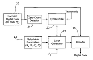
- FIG. 2 is a block diagram of a preferred embodiment of a clock recovery apparatus of the present invention.
- FIG. 3 is a block diagram of a synchronizer of the present invention.
- FIG. 4 is a block diagram of a clock generator of the present invention.
- FIG. 5 shows example waveforms within the synchronizer for generating a sync signal.
- FIG. 6 shows an accumulated error signal used by the clock generator to select a variable clock period.
- FIG. 7 shows sample values for parameters used in the clock generator to regenerate a data clock signal.
- FIG. 1( a ) shows an RDS data stream as generated prior to transmission using bi-phase encoding wherein a “1” bit is represented as a single cycle with a first phase (e.g., a negative-going transition at the midpoint of the bit period) and a “0” bit is represented as a single cycle with a second phase which is reversed from the first phase (e.g., a positive-going transition at the midpoint).
- a zero-crossing or edge occurs at the beginning, midpoint, and ending of a bit period.
- the binary signal changes from one bit value to the other, there is no zero-crossing or edge at the beginning of the corresponding bit period.
- FIG. 1( b ) shows an ideal clock timing signal corresponding to the timing used to generate the bi-phase encoded data stream and having an ideal bit time slot or bit period P i .
- FIG. 1( c ) shows a sampling frequency that is selected to be an integer multiple of the ideal bit rate or bit frequency so that a whole number of sampling frequency timing pulses are produced for each cycle of the ideal bit timing signal. For example, a sampling frequency that is 8 times the bit rate is shown (i.e., 8 sample pulses occur for each bit period).
- a free running counter driven at the sampling frequency can substantially match the frequency of the original clock timing signal.
- phase of the recovered clock signal by several different methods, including pattern matching (e.g., finding sample windows with equal numbers of positive and negative date sample values) and zero crossing detection (e.g., finding the sample position within the clock cycle that contains the most zero crossings).
- pattern matching e.g., finding sample windows with equal numbers of positive and negative date sample values
- zero crossing detection e.g., finding the sample position within the clock cycle that contains the most zero crossings.
- the sampling frequency used in the receiver was an integer multiple of the data bit rate.
- a data bit rate R b of an RDS or RDBS signal is 1,187.5 Hz.
- Prior art receivers have typically used a sampling frequency of 9.5 kHz, so that 8 samples were counted out per RDS bit. Because of other considerations in the design of a receiver, it may be desirable to use a sampling frequency other than a multiple of 1,187.5 Hz.
- a sampling frequency F s of 10.546874 kHz could be used which results in a ratio of F s to R b of 8.8815789. Since a clock counter can only count integer number, however, it is not possible to count an exact period of the data signal.
- the present invention adopts a variable clock period by dynamically alternating the clock count between an integer number sample count S just greater than and just lower than the ratio.
- the number of samples counted out during the recovered clock period alternates between an upper count value S u of 9 samples and a lower count value S l of 8 samples as is shown in FIG. 1( d ).
- a variable clock period is provided with an average length that is substantially equal to the data bit period (i.e., the average value of S approaches the ratio F s /R b ).
- the resulting error between the recovered clock signal and the ideal clock signal is always less than one sample period.
- the recovered clock signal is properly phased (i.e., synchronized), it can satisfactorily be used to decode the digital data signal.
- the present invention synchronizes the clock signal based on detecting a zero crossing that occurs at the middle of a bit period.
- an input pulse signal comprising pulses 10 is generated based on zero crossings of the data signal of FIG. 1( a ).
- pulses 10 are more closely spaced because zero crossings occur at the beginning, middle and ends of a bit period.
- the bit value changes, there is no zero crossing at the beginning of the new bit period, creating a longer interval between pulses 10 . This longer interval is detected and the next pulse 10 is known to occur at the middle of a bit period, thereby allowing synchronization.
- a receiver front end 20 provides an encoded digital data signal having a bit rate R b .
- Front end 20 may comprise a radio tuner and demodulator for receiving an RDS broadcast, for example.
- the encoded digital data signal is provided to a zero-crossing detector 21 and to a decoder 25 .
- Input pulses from zero-crossing detector 21 are provided to a synchronizer 22 .
- Based on certain thresholds also provided to synchronizer 22 a synchronization or sync signal is provided to a clock generator 23 .
- a programmable memory 24 contains selectable parameters used by clock generator 23 to generate almost any arbitrary recovered clock frequency based on a sampling frequency F s which may have almost any arbitrary frequency.
- the selectable parameters include upper and lower count values S u and S l and duty cycle limits N u and N l described below.
- clock generator 23 regenerates the clock timing signal which is provided to decoder 25 to regenerate the original binary data stream.
- Synchronizer 22 is shown in greater detail in FIG. 3 .
- Input pulses are input to a pulse accumulator 30 which maintains an integer pulse count of the number of input pulses that have occurred since the last time accumulator 30 was reset.
- the pulse count is provided to one input of a comparison block 31 for comparing the pulse count to a threshold.
- Either a fast re-sync threshold or a slow re-sync threshold is provided to the remaining input of comparison block 31 via a selector switch 32 .
- Switch 32 is controlled by a threshold decision block 33 which receives the sync signal, a power-up/reset signal, and a signal-quality signal.
- the slow re-sync threshold is used since a reliable synchronization is achieved.
- the fast re-synch threshold with a lower count value is used so that re-synchronization happens sooner.
- the signal-quality signal may, for example, be obtained from the date decoder in response to the detected bit errors in the finally decoded digital signal.
- Threshold decision block 33 uses the sync signal to gate any change in the setting of switch 32 .
- the input pulse signal is also provided to a sample accumulator 34 which counts the sample frequency F s between adjacent input pulses (i.e., the sample count is reset by each input pulse).
- the sample count is provided to one input of a comparison block 35 which receives a sample threshold at its other input.
- the sample threshold signifies the time (i.e., number of samples counted) between zero crossings when a phase reversal (i.e., change of bit value) occurs in the data signal.
- the sample threshold has an integer value between the number of samples counted during a bit period (i.e., F s /R b ) and the number counted during one-half a bit period.
- F s /R b equals 8.8815789
- the present invention generates a sync signal or sync pulse when both the pulse count is greater than the re-sync threshold currently selected and the sample count is greater than the sample threshold.
- the outputs of comparison blocks 31 and 35 are coupled to respective inputs of an AND-gate 36 .
- a third input of AND-gate 36 receives the input pulse signal so that the sync signal is triggered at the appropriate time of a zero crossing.
- FIG. 5 Waveforms relating to the synchronization function are shown in FIG. 5 .
- the contents of the pulse accumulator are shown in FIG. 5( a ) as it increases from being initialized a zero.
- a pulse threshold is shown for providing relatively fast resynchronization.
- FIG. 5( b ) shows the contents of the sample accumulator which counts between the input pulses.
- the sample count is incremented beyond the sample threshold (which ensures that the next input pulse coincides with the center of a bit period).
- the sync signal pulse is produced as shown in FIG. 5( c ).
- Clock generator 23 is shown in greater detail in FIG. 4 .
- the sync signal is provided to a clock counter 40 and a count selection block 41 .
- Clock counter 40 produces a cyclical count according to the current count value S (the actual count typically runs from zero to S ⁇ 1) at the rate determined by sampling frequency F s .
- Preconfigured count values S u and S l are provided to respective inputs of a selector switch 42 controlled by count selection block 41 .
- the selected count value is output by switch 42 to clock counter 40 , a subtracting output of a summer 43 , and a logic controller 47 .
- An adding input of summer 43 receives a sample rate/data rate ratio D s (equal to F s /R b ).
- the output of summer 43 is connected to an input of an error comparison block 44 and to the input of a unit delay block 45 .
- the output of unit delay block 45 is connected to a third input of summer 43 .
- An error threshold is provided to the remaining (e.g., inverting) input of comparison block 44 .
- the output of comparison block 44 is coupled to count selection block 41 to provide a high logic level signal when the accumulated error (i.e., the sum of any previous error and the current error resulting from the difference between the ideal bit period of the data signal and the variable clock period corresponding to the current value of S) is greater than the error threshold.
- the error threshold corresponds to the number of sample periods by which the regenerated clock signal is allowed to drift from the ideal value before the count value is switched in order to change the direction of the error growth.
- the upper or lower count value that is closer to the value of D s is preferably used the majority of the time so that the error accumulates more slowly.
- the closer count value is selected by selection block 41 .
- the selection of count value S as a function of the accumulated error versus the error threshold is shown in FIG. 6 .
- an error threshold value close to, but preferably not equal to, one half is selected in order to provide good tracking of the regenerated clock signal to the ideal signal. If the fractional part of D s is greater than 0.5, then the error threshold is preferably also assigned a value greater than 0.5 (and if the fractional part is less than 0.5 then the error threshold is also less than 0.5).
- count selection block 41 initially selects upper count value S u (e.g., 9) to be used. An error threshold of 0.6 is used. Once the beginning of a regenerated clock cycle is late by 0.6 sample periods, count selection block 41 selects lower count value S l (e.g., 8) so that the next regenerated clock cycle begins early.
- the regenerated clock signal from clock counter 40 which is synchronized (i.e., begins a new counting cycle at zero) at the midpoint of the data bit period is provided to a clock signal generator block 46 which encodes the clock count into a binary recovered clock signal.
- the alignment of the regenerated clock signal to the counting cycle of clock counter 40 and the duty cycle of the regenerated clock signal are controlled by logic controller 47 through the setting of duty cycle limits N u and N l . More specifically, clock signal generator 46 produces a square-wave clock signal (e.g., varying between high and low logic levels) that is encoded at a high level when the count output by clock counter 40 has a value from N l to N u , inclusive.
- any arbitrary duty cycle or any phase relationship between the clock count can be obtained.
- the values of N l and N u would span the second half of a counting cycle of clock counter 40 (e.g., a value of 4 for N l and a value of 7 for N u when the value of the clock count S is 8).
- FIG. 7 shows various signal values during operation of the present invention using the parameters of the above numerical example for successive sample periods moving toward the right in FIG. 7 .
- the count value S is initially the upper value 9, so that the clock count is cycling from 0 through 8.
- the recovered clock signal has a value of zero for the first four sample time slots and a value of one for the next five sample time slots.
- the count value S is switched to the lower value of 8.
- the value of N u is switched to 7 to take into account the shorter counting cycle.
- This second counting cycle ends when the count reaches 7, at which time the error has been reduced to an amount below the error threshold. Therefore, count value S is switched back to its upper value of 9 and N u is changed back to 8. After a few counts, a sync signal occurs and the clock count is reinitiated at zero.
Abstract
Description
Claims (17)
Priority Applications (3)
| Application Number | Priority Date | Filing Date | Title |
|---|---|---|---|
| US10/284,231 US7072431B2 (en) | 2002-10-30 | 2002-10-30 | Clock timing recovery using arbitrary sampling frequency |
| GB0323312A GB2394870B (en) | 2002-10-30 | 2003-10-06 | Clock timing recovery using arbitrary sampling frequency |
| DE10351432A DE10351432B4 (en) | 2002-10-30 | 2003-10-27 | Timing regeneration using an arbitrary sampling frequency |
Applications Claiming Priority (1)
| Application Number | Priority Date | Filing Date | Title |
|---|---|---|---|
| US10/284,231 US7072431B2 (en) | 2002-10-30 | 2002-10-30 | Clock timing recovery using arbitrary sampling frequency |
Publications (2)
| Publication Number | Publication Date |
|---|---|
| US20040086067A1 US20040086067A1 (en) | 2004-05-06 |
| US7072431B2 true US7072431B2 (en) | 2006-07-04 |
Family
ID=29420200
Family Applications (1)
| Application Number | Title | Priority Date | Filing Date |
|---|---|---|---|
| US10/284,231 Active 2024-12-08 US7072431B2 (en) | 2002-10-30 | 2002-10-30 | Clock timing recovery using arbitrary sampling frequency |
Country Status (3)
| Country | Link |
|---|---|
| US (1) | US7072431B2 (en) |
| DE (1) | DE10351432B4 (en) |
| GB (1) | GB2394870B (en) |
Cited By (5)
| Publication number | Priority date | Publication date | Assignee | Title |
|---|---|---|---|---|
| US20040057734A1 (en) * | 2002-09-25 | 2004-03-25 | Lucent Technologies, Inc. | Method and system for reducing transmission penalties associated with ghost pulses |
| US20120087350A1 (en) * | 2010-10-06 | 2012-04-12 | John Peter Norair | Method and Apparatus for Low-Power, Long-Range Networking |
| US8929961B2 (en) | 2011-07-15 | 2015-01-06 | Blackbird Technology Holdings, Inc. | Protective case for adding wireless functionality to a handheld electronic device |
| US9166894B2 (en) | 2011-03-02 | 2015-10-20 | Blackbird Technology Holdings, Inc. | Method and apparatus for rapid group synchronization |
| US9357425B2 (en) | 2010-10-06 | 2016-05-31 | Blackbird Technology Holdings, Inc. | Method and apparatus for adaptive searching of distributed datasets |
Families Citing this family (3)
| Publication number | Priority date | Publication date | Assignee | Title |
|---|---|---|---|---|
| US7149265B2 (en) * | 2003-05-16 | 2006-12-12 | Visteon Global Technologies, Inc. | Timing recovery loop with non-integer length |
| CN110061733B (en) * | 2019-04-19 | 2023-04-04 | 苏州瑞迈斯医疗科技有限公司 | Pulse signal counting method, pulse signal reconstruction method and chip |
| TWI703849B (en) | 2019-08-06 | 2020-09-01 | 瑞昱半導體股份有限公司 | Smart phase switching method and smart phase switching system |
Citations (14)
| Publication number | Priority date | Publication date | Assignee | Title |
|---|---|---|---|---|
| US3805180A (en) | 1972-12-27 | 1974-04-16 | A Widmer | Binary-coded signal timing recovery circuit |
| US4330759A (en) | 1980-03-05 | 1982-05-18 | Bell Telephone Laboratories, Incorporated | Apparatus for generating synchronized timing pulses from binary data signals |
| EP0311974A2 (en) | 1987-10-14 | 1989-04-19 | National Semiconductor Corporation | Timing recovery system using bipolar-pattern center estimator |
| US5199046A (en) | 1991-09-09 | 1993-03-30 | Codex Corporation | First and second digital rate converter synchronization device and method |
| US5216717A (en) | 1990-03-02 | 1993-06-01 | Telediffusion De France | Frequency modulation broadcast transmitter synchronization method |
| US5636249A (en) | 1994-12-08 | 1997-06-03 | Sgs-Thomson Microelectronics Gmbh | Method of and apparatus for phase synchronization with an RDS signal |
| US5682605A (en) * | 1994-11-14 | 1997-10-28 | 989008 Ontario Inc. | Wireless communication system |
| EP0877506A2 (en) | 1997-05-02 | 1998-11-11 | Kokusai Denshin Denwa Co., Ltd | Timing recovery and tracking method and apparatus for data signals |
| US5928293A (en) | 1996-04-30 | 1999-07-27 | Motorola, Inc. | Method for generating a clock signal for use in a data receiver, clock generator, data receiver and remote controlled access system for vehicles |
| US5970093A (en) | 1996-01-23 | 1999-10-19 | Tiernan Communications, Inc. | Fractionally-spaced adaptively-equalized self-recovering digital receiver for amplitude-Phase modulated signals |
| US5969631A (en) * | 1996-06-14 | 1999-10-19 | Temic Telefunken Microelectronic Gmbh | Method and control system for the synchronized transmission of digital data |
| US6178213B1 (en) | 1998-08-25 | 2001-01-23 | Vitesse Semiconductor Corporation | Adaptive data recovery system and methods |
| US6229862B1 (en) | 1991-07-02 | 2001-05-08 | British Telecommunications Public Limited Company | Selective clock recovery from portions of digital data signal best suited therefor |
| US6665359B1 (en) * | 1999-10-28 | 2003-12-16 | Stmicroelectronics, Inc. | Digital data separator |
Family Cites Families (2)
| Publication number | Priority date | Publication date | Assignee | Title |
|---|---|---|---|---|
| DE3728655A1 (en) * | 1987-08-27 | 1989-03-09 | Thomson Brandt Gmbh | METHOD AND / OR DEVICE FOR DEMODULATING A BIPHASE SIGNAL |
| DE10112638A1 (en) * | 2001-03-16 | 2002-09-26 | Harman Becker Automotive Sys | Method and circuit arrangement for generating the RDS bit clock |
-
2002
- 2002-10-30 US US10/284,231 patent/US7072431B2/en active Active
-
2003
- 2003-10-06 GB GB0323312A patent/GB2394870B/en not_active Expired - Fee Related
- 2003-10-27 DE DE10351432A patent/DE10351432B4/en not_active Expired - Fee Related
Patent Citations (15)
| Publication number | Priority date | Publication date | Assignee | Title |
|---|---|---|---|---|
| US3805180A (en) | 1972-12-27 | 1974-04-16 | A Widmer | Binary-coded signal timing recovery circuit |
| US4330759A (en) | 1980-03-05 | 1982-05-18 | Bell Telephone Laboratories, Incorporated | Apparatus for generating synchronized timing pulses from binary data signals |
| EP0311974A2 (en) | 1987-10-14 | 1989-04-19 | National Semiconductor Corporation | Timing recovery system using bipolar-pattern center estimator |
| US5216717A (en) | 1990-03-02 | 1993-06-01 | Telediffusion De France | Frequency modulation broadcast transmitter synchronization method |
| US6229862B1 (en) | 1991-07-02 | 2001-05-08 | British Telecommunications Public Limited Company | Selective clock recovery from portions of digital data signal best suited therefor |
| US5199046A (en) | 1991-09-09 | 1993-03-30 | Codex Corporation | First and second digital rate converter synchronization device and method |
| US5682605A (en) * | 1994-11-14 | 1997-10-28 | 989008 Ontario Inc. | Wireless communication system |
| US5636249A (en) | 1994-12-08 | 1997-06-03 | Sgs-Thomson Microelectronics Gmbh | Method of and apparatus for phase synchronization with an RDS signal |
| US5970093A (en) | 1996-01-23 | 1999-10-19 | Tiernan Communications, Inc. | Fractionally-spaced adaptively-equalized self-recovering digital receiver for amplitude-Phase modulated signals |
| US6141378A (en) | 1996-01-23 | 2000-10-31 | Tiernan Communications, Inc. | Fractionally-spaced adaptively-equalized self-recovering digital receiver for amplitude-phase modulated signals |
| US5928293A (en) | 1996-04-30 | 1999-07-27 | Motorola, Inc. | Method for generating a clock signal for use in a data receiver, clock generator, data receiver and remote controlled access system for vehicles |
| US5969631A (en) * | 1996-06-14 | 1999-10-19 | Temic Telefunken Microelectronic Gmbh | Method and control system for the synchronized transmission of digital data |
| EP0877506A2 (en) | 1997-05-02 | 1998-11-11 | Kokusai Denshin Denwa Co., Ltd | Timing recovery and tracking method and apparatus for data signals |
| US6178213B1 (en) | 1998-08-25 | 2001-01-23 | Vitesse Semiconductor Corporation | Adaptive data recovery system and methods |
| US6665359B1 (en) * | 1999-10-28 | 2003-12-16 | Stmicroelectronics, Inc. | Digital data separator |
Cited By (10)
| Publication number | Priority date | Publication date | Assignee | Title |
|---|---|---|---|---|
| US20040057734A1 (en) * | 2002-09-25 | 2004-03-25 | Lucent Technologies, Inc. | Method and system for reducing transmission penalties associated with ghost pulses |
| US20120087350A1 (en) * | 2010-10-06 | 2012-04-12 | John Peter Norair | Method and Apparatus for Low-Power, Long-Range Networking |
| US9042353B2 (en) * | 2010-10-06 | 2015-05-26 | Blackbird Technology Holdings, Inc. | Method and apparatus for low-power, long-range networking |
| US9357425B2 (en) | 2010-10-06 | 2016-05-31 | Blackbird Technology Holdings, Inc. | Method and apparatus for adaptive searching of distributed datasets |
| US9379808B2 (en) | 2010-10-06 | 2016-06-28 | Blackbird Technology Holdings, Inc. | Method and apparatus for low-power, long-range networking |
| US9166894B2 (en) | 2011-03-02 | 2015-10-20 | Blackbird Technology Holdings, Inc. | Method and apparatus for rapid group synchronization |
| US9325634B2 (en) | 2011-03-02 | 2016-04-26 | Blackbird Technology Holdings, Inc. | Method and apparatus for adaptive traffic management in a resource-constrained network |
| US9414342B2 (en) | 2011-03-02 | 2016-08-09 | Blackbird Technology Holdings, Inc. | Method and apparatus for query-based congestion control |
| US8929961B2 (en) | 2011-07-15 | 2015-01-06 | Blackbird Technology Holdings, Inc. | Protective case for adding wireless functionality to a handheld electronic device |
| US9425847B2 (en) | 2011-07-15 | 2016-08-23 | Blackbird Technology Holdings, Inc. | Protective case for adding wireless functionality to a handheld electronic device |
Also Published As
| Publication number | Publication date |
|---|---|
| US20040086067A1 (en) | 2004-05-06 |
| DE10351432A1 (en) | 2004-05-19 |
| GB0323312D0 (en) | 2003-11-05 |
| GB2394870A (en) | 2004-05-05 |
| GB2394870B (en) | 2005-02-02 |
| DE10351432B4 (en) | 2006-06-08 |
Similar Documents
| Publication | Publication Date | Title |
|---|---|---|
| KR960016644B1 (en) | Method and apparatus for transmission path delay measurment using adaptive demodulation | |
| US7466772B2 (en) | Decoding coded data streams | |
| JP3307527B2 (en) | PPM demodulator | |
| WO1998016040A1 (en) | Method and apparatus for decoding of spdif or aes/ebu digital audio data | |
| JP4290886B2 (en) | Method and apparatus for providing robust synchronization of a radio transceiver | |
| US7072431B2 (en) | Clock timing recovery using arbitrary sampling frequency | |
| US6768433B1 (en) | Method and system for decoding biphase-mark encoded data | |
| JP3431743B2 (en) | Method and apparatus for performing RDS phase synchronization on receiver side | |
| US7149265B2 (en) | Timing recovery loop with non-integer length | |
| US5274672A (en) | Optimized clock recovery for an MSK system | |
| JPH08279804A (en) | Method and device for phasic synchronization with rds signal | |
| US6933866B1 (en) | Variable data rate receiver | |
| EP0803999B1 (en) | Demodulator device for data carried by subcarriers | |
| EP0930713B1 (en) | Decoding of a biphase modulated bitstream and relative selfsynchronizing frequency divider with noninteger ratio | |
| JP2001522577A (en) | Clock recovery circuit and receiver having clock recovery circuit | |
| EP0600408B1 (en) | Method and apparatus for clock synchronization | |
| US5311559A (en) | Apparatus for correcting waveform distortion | |
| JPH09289465A (en) | Rds signal discrimination device | |
| JP2506805B2 (en) | Data processing device in RDS receiver | |
| KR100192451B1 (en) | Method and apparatus of checking transmission mode in digital audio broadcasting | |
| JP2556125B2 (en) | Data demodulator | |
| US5802067A (en) | FM multiplex broadcast receiving circuit for detecting presence or absence of multiplex information | |
| US7466770B2 (en) | Adaptive pulse width discrimination using an asynchronous clock | |
| JP3856586B2 (en) | Synchronization judgment device | |
| JP2506811B2 (en) | Data processing method in RDS receiver |
Legal Events
| Date | Code | Title | Description |
|---|---|---|---|
| AS | Assignment |
Owner name: VISTEON GLOBAL TECHNOLOGIES, INC., MICHIGAN Free format text: ASSIGNMENT OF ASSIGNORS INTEREST;ASSIGNORS:WANG, VINCENT;WHIKEHART, J. WILLIAM;WHITECAR, JOHN E.;REEL/FRAME:013454/0492 Effective date: 20021029 |
|
| STCF | Information on status: patent grant |
Free format text: PATENTED CASE |
|
| AS | Assignment |
Owner name: JPMORGAN CHASE BANK, N.A., AS ADMINISTRATIVE AGENT Free format text: SECURITY AGREEMENT;ASSIGNOR:VISTEON GLOBAL TECHNOLOGIES, INC.;REEL/FRAME:020497/0733 Effective date: 20060613 |
|
| AS | Assignment |
Owner name: JPMORGAN CHASE BANK, TEXAS Free format text: SECURITY INTEREST;ASSIGNOR:VISTEON GLOBAL TECHNOLOGIES, INC.;REEL/FRAME:022368/0001 Effective date: 20060814 Owner name: JPMORGAN CHASE BANK,TEXAS Free format text: SECURITY INTEREST;ASSIGNOR:VISTEON GLOBAL TECHNOLOGIES, INC.;REEL/FRAME:022368/0001 Effective date: 20060814 |
|
| AS | Assignment |
Owner name: WILMINGTON TRUST FSB, AS ADMINISTRATIVE AGENT, MIN Free format text: ASSIGNMENT OF SECURITY INTEREST IN PATENTS;ASSIGNOR:JPMORGAN CHASE BANK, N.A., AS ADMINISTRATIVE AGENT;REEL/FRAME:022575/0186 Effective date: 20090415 Owner name: WILMINGTON TRUST FSB, AS ADMINISTRATIVE AGENT,MINN Free format text: ASSIGNMENT OF SECURITY INTEREST IN PATENTS;ASSIGNOR:JPMORGAN CHASE BANK, N.A., AS ADMINISTRATIVE AGENT;REEL/FRAME:022575/0186 Effective date: 20090415 |
|
| AS | Assignment |
Owner name: THE BANK OF NEW YORK MELLON, AS ADMINISTRATIVE AGE Free format text: ASSIGNMENT OF PATENT SECURITY INTEREST;ASSIGNOR:JPMORGAN CHASE BANK, N.A., A NATIONAL BANKING ASSOCIATION;REEL/FRAME:022974/0057 Effective date: 20090715 |
|
| FPAY | Fee payment |
Year of fee payment: 4 |
|
| AS | Assignment |
Owner name: VISTEON GLOBAL TECHNOLOGIES, INC., MICHIGAN Free format text: RELEASE BY SECURED PARTY AGAINST SECURITY INTEREST IN PATENTS RECORDED AT REEL 022974 FRAME 0057;ASSIGNOR:THE BANK OF NEW YORK MELLON;REEL/FRAME:025095/0711 Effective date: 20101001 |
|
| AS | Assignment |
Owner name: VISTEON GLOBAL TECHNOLOGIES, INC., MICHIGAN Free format text: RELEASE BY SECURED PARTY AGAINST SECURITY INTEREST IN PATENTS RECORDED AT REEL 022575 FRAME 0186;ASSIGNOR:WILMINGTON TRUST FSB, AS ADMINISTRATIVE AGENT;REEL/FRAME:025105/0201 Effective date: 20101001 |
|
| AS | Assignment |
Owner name: MORGAN STANLEY SENIOR FUNDING, INC., AS AGENT, NEW Free format text: SECURITY AGREEMENT;ASSIGNORS:VISTEON CORPORATION;VC AVIATION SERVICES, LLC;VISTEON ELECTRONICS CORPORATION;AND OTHERS;REEL/FRAME:025241/0317 Effective date: 20101007 Owner name: MORGAN STANLEY SENIOR FUNDING, INC., AS AGENT, NEW Free format text: SECURITY AGREEMENT (REVOLVER);ASSIGNORS:VISTEON CORPORATION;VC AVIATION SERVICES, LLC;VISTEON ELECTRONICS CORPORATION;AND OTHERS;REEL/FRAME:025238/0298 Effective date: 20101001 |
|
| AS | Assignment |
Owner name: VISTEON GLOBAL TREASURY, INC., MICHIGAN Free format text: RELEASE BY SECURED PARTY AGAINST SECURITY INTEREST IN PATENTS ON REEL 025241 FRAME 0317;ASSIGNOR:MORGAN STANLEY SENIOR FUNDING, INC.;REEL/FRAME:026178/0412 Effective date: 20110406 Owner name: VC AVIATION SERVICES, LLC, MICHIGAN Free format text: RELEASE BY SECURED PARTY AGAINST SECURITY INTEREST IN PATENTS ON REEL 025241 FRAME 0317;ASSIGNOR:MORGAN STANLEY SENIOR FUNDING, INC.;REEL/FRAME:026178/0412 Effective date: 20110406 Owner name: VISTEON ELECTRONICS CORPORATION, MICHIGAN Free format text: RELEASE BY SECURED PARTY AGAINST SECURITY INTEREST IN PATENTS ON REEL 025241 FRAME 0317;ASSIGNOR:MORGAN STANLEY SENIOR FUNDING, INC.;REEL/FRAME:026178/0412 Effective date: 20110406 Owner name: VISTEON CORPORATION, MICHIGAN Free format text: RELEASE BY SECURED PARTY AGAINST SECURITY INTEREST IN PATENTS ON REEL 025241 FRAME 0317;ASSIGNOR:MORGAN STANLEY SENIOR FUNDING, INC.;REEL/FRAME:026178/0412 Effective date: 20110406 Owner name: VISTEON GLOBAL TECHNOLOGIES, INC., MICHIGAN Free format text: RELEASE BY SECURED PARTY AGAINST SECURITY INTEREST IN PATENTS ON REEL 025241 FRAME 0317;ASSIGNOR:MORGAN STANLEY SENIOR FUNDING, INC.;REEL/FRAME:026178/0412 Effective date: 20110406 Owner name: VISTEON EUROPEAN HOLDING, INC., MICHIGAN Free format text: RELEASE BY SECURED PARTY AGAINST SECURITY INTEREST IN PATENTS ON REEL 025241 FRAME 0317;ASSIGNOR:MORGAN STANLEY SENIOR FUNDING, INC.;REEL/FRAME:026178/0412 Effective date: 20110406 Owner name: VISTEON SYSTEMS, LLC, MICHIGAN Free format text: RELEASE BY SECURED PARTY AGAINST SECURITY INTEREST IN PATENTS ON REEL 025241 FRAME 0317;ASSIGNOR:MORGAN STANLEY SENIOR FUNDING, INC.;REEL/FRAME:026178/0412 Effective date: 20110406 Owner name: VISTEON INTERNATIONAL HOLDINGS, INC., MICHIGAN Free format text: RELEASE BY SECURED PARTY AGAINST SECURITY INTEREST IN PATENTS ON REEL 025241 FRAME 0317;ASSIGNOR:MORGAN STANLEY SENIOR FUNDING, INC.;REEL/FRAME:026178/0412 Effective date: 20110406 Owner name: VISTEON INTERNATIONAL BUSINESS DEVELOPMENT, INC., Free format text: RELEASE BY SECURED PARTY AGAINST SECURITY INTEREST IN PATENTS ON REEL 025241 FRAME 0317;ASSIGNOR:MORGAN STANLEY SENIOR FUNDING, INC.;REEL/FRAME:026178/0412 Effective date: 20110406 |
|
| FPAY | Fee payment |
Year of fee payment: 8 |
|
| AS | Assignment |
Owner name: CITIBANK., N.A., AS ADMINISTRATIVE AGENT, NEW YORK Free format text: SECURITY INTEREST;ASSIGNORS:VISTEON CORPORATION, AS GRANTOR;VISTEON GLOBAL TECHNOLOGIES, INC., AS GRANTOR;REEL/FRAME:032713/0065 Effective date: 20140409 |
|
| AS | Assignment |
Owner name: VISTEON ELECTRONICS CORPORATION, MICHIGAN Free format text: RELEASE OF SECURITY INTEREST IN INTELLECTUAL PROPERTY;ASSIGNOR:MORGAN STANLEY SENIOR FUNDING, INC.;REEL/FRAME:033107/0717 Effective date: 20140409 Owner name: VISTEON EUROPEAN HOLDINGS, INC., MICHIGAN Free format text: RELEASE OF SECURITY INTEREST IN INTELLECTUAL PROPERTY;ASSIGNOR:MORGAN STANLEY SENIOR FUNDING, INC.;REEL/FRAME:033107/0717 Effective date: 20140409 Owner name: VISTEON GLOBAL TREASURY, INC., MICHIGAN Free format text: RELEASE OF SECURITY INTEREST IN INTELLECTUAL PROPERTY;ASSIGNOR:MORGAN STANLEY SENIOR FUNDING, INC.;REEL/FRAME:033107/0717 Effective date: 20140409 Owner name: VISTEON INTERNATIONAL BUSINESS DEVELOPMENT, INC., Free format text: RELEASE OF SECURITY INTEREST IN INTELLECTUAL PROPERTY;ASSIGNOR:MORGAN STANLEY SENIOR FUNDING, INC.;REEL/FRAME:033107/0717 Effective date: 20140409 Owner name: VISTEON SYSTEMS, LLC, MICHIGAN Free format text: RELEASE OF SECURITY INTEREST IN INTELLECTUAL PROPERTY;ASSIGNOR:MORGAN STANLEY SENIOR FUNDING, INC.;REEL/FRAME:033107/0717 Effective date: 20140409 Owner name: VISTEON INTERNATIONAL HOLDINGS, INC., MICHIGAN Free format text: RELEASE OF SECURITY INTEREST IN INTELLECTUAL PROPERTY;ASSIGNOR:MORGAN STANLEY SENIOR FUNDING, INC.;REEL/FRAME:033107/0717 Effective date: 20140409 Owner name: VC AVIATION SERVICES, LLC, MICHIGAN Free format text: RELEASE OF SECURITY INTEREST IN INTELLECTUAL PROPERTY;ASSIGNOR:MORGAN STANLEY SENIOR FUNDING, INC.;REEL/FRAME:033107/0717 Effective date: 20140409 Owner name: VISTEON GLOBAL TECHNOLOGIES, INC., MICHIGAN Free format text: RELEASE OF SECURITY INTEREST IN INTELLECTUAL PROPERTY;ASSIGNOR:MORGAN STANLEY SENIOR FUNDING, INC.;REEL/FRAME:033107/0717 Effective date: 20140409 Owner name: VISTEON CORPORATION, MICHIGAN Free format text: RELEASE OF SECURITY INTEREST IN INTELLECTUAL PROPERTY;ASSIGNOR:MORGAN STANLEY SENIOR FUNDING, INC.;REEL/FRAME:033107/0717 Effective date: 20140409 |
|
| FEPP | Fee payment procedure |
Free format text: PAYOR NUMBER ASSIGNED (ORIGINAL EVENT CODE: ASPN); ENTITY STATUS OF PATENT OWNER: LARGE ENTITY |
|
| FEPP | Fee payment procedure |
Free format text: 11.5 YR SURCHARGE- LATE PMT W/IN 6 MO, LARGE ENTITY (ORIGINAL EVENT CODE: M1556) |
|
| MAFP | Maintenance fee payment |
Free format text: PAYMENT OF MAINTENANCE FEE, 12TH YEAR, LARGE ENTITY (ORIGINAL EVENT CODE: M1553) Year of fee payment: 12 |