US7280615B2 - Method for making a clear channel assessment in a wireless network - Google Patents
Method for making a clear channel assessment in a wireless network Download PDFInfo
- Publication number
- US7280615B2 US7280615B2 US10/677,753 US67775303A US7280615B2 US 7280615 B2 US7280615 B2 US 7280615B2 US 67775303 A US67775303 A US 67775303A US 7280615 B2 US7280615 B2 US 7280615B2
- Authority
- US
- United States
- Prior art keywords
- clear channel
- channel assessment
- signal
- synchronized
- wireless network
- Prior art date
- Legal status (The legal status is an assumption and is not a legal conclusion. Google has not performed a legal analysis and makes no representation as to the accuracy of the status listed.)
- Expired - Fee Related, expires
Links
- 238000000034 method Methods 0.000 title claims abstract description 101
- 230000001360 synchronised effect Effects 0.000 claims abstract description 74
- 238000001514 detection method Methods 0.000 claims abstract description 15
- 238000001914 filtration Methods 0.000 claims description 15
- 230000003321 amplification Effects 0.000 claims description 9
- 238000003199 nucleic acid amplification method Methods 0.000 claims description 9
- 230000005540 biological transmission Effects 0.000 description 71
- 238000010586 diagram Methods 0.000 description 38
- 230000003595 spectral effect Effects 0.000 description 38
- 238000001228 spectrum Methods 0.000 description 31
- 230000008569 process Effects 0.000 description 16
- 230000000875 corresponding effect Effects 0.000 description 15
- 230000008901 benefit Effects 0.000 description 14
- 239000000047 product Substances 0.000 description 11
- 238000000354 decomposition reaction Methods 0.000 description 10
- 238000013461 design Methods 0.000 description 10
- 238000004891 communication Methods 0.000 description 9
- 238000004458 analytical method Methods 0.000 description 7
- 238000009826 distribution Methods 0.000 description 7
- 230000000694 effects Effects 0.000 description 7
- 238000012545 processing Methods 0.000 description 7
- 230000010363 phase shift Effects 0.000 description 6
- 238000000926 separation method Methods 0.000 description 6
- 238000012549 training Methods 0.000 description 6
- 230000003111 delayed effect Effects 0.000 description 5
- 230000011664 signaling Effects 0.000 description 5
- 238000013459 approach Methods 0.000 description 4
- 229910002056 binary alloy Inorganic materials 0.000 description 4
- 238000012937 correction Methods 0.000 description 4
- 238000005562 fading Methods 0.000 description 4
- 230000004044 response Effects 0.000 description 4
- 230000008859 change Effects 0.000 description 3
- 238000005516 engineering process Methods 0.000 description 3
- 238000013507 mapping Methods 0.000 description 3
- 238000005259 measurement Methods 0.000 description 3
- 238000004088 simulation Methods 0.000 description 3
- 238000012546 transfer Methods 0.000 description 3
- 239000013598 vector Substances 0.000 description 3
- 238000006243 chemical reaction Methods 0.000 description 2
- 230000003993 interaction Effects 0.000 description 2
- 238000010183 spectrum analysis Methods 0.000 description 2
- 238000003860 storage Methods 0.000 description 2
- 238000013519 translation Methods 0.000 description 2
- RYQHXWDFNMMYSD-UHFFFAOYSA-O (1-methylpyridin-4-ylidene)methyl-oxoazanium Chemical compound CN1C=CC(=C[NH+]=O)C=C1 RYQHXWDFNMMYSD-UHFFFAOYSA-O 0.000 description 1
- 239000002131 composite material Substances 0.000 description 1
- 230000001276 controlling effect Effects 0.000 description 1
- 230000002596 correlated effect Effects 0.000 description 1
- 230000001066 destructive effect Effects 0.000 description 1
- 230000003467 diminishing effect Effects 0.000 description 1
- 230000007613 environmental effect Effects 0.000 description 1
- 230000007274 generation of a signal involved in cell-cell signaling Effects 0.000 description 1
- 230000000977 initiatory effect Effects 0.000 description 1
- 238000004519 manufacturing process Methods 0.000 description 1
- 229940050561 matrix product Drugs 0.000 description 1
- 238000012986 modification Methods 0.000 description 1
- 230000004048 modification Effects 0.000 description 1
- 230000006855 networking Effects 0.000 description 1
- 230000000737 periodic effect Effects 0.000 description 1
- JBKPUQTUERUYQE-UHFFFAOYSA-O pralidoxime Chemical compound C[N+]1=CC=CC=C1\C=N\O JBKPUQTUERUYQE-UHFFFAOYSA-O 0.000 description 1
- 230000009467 reduction Effects 0.000 description 1
- 230000003252 repetitive effect Effects 0.000 description 1
- 230000002441 reversible effect Effects 0.000 description 1
- 239000004065 semiconductor Substances 0.000 description 1
- 238000009987 spinning Methods 0.000 description 1
- 239000013589 supplement Substances 0.000 description 1
- 230000036962 time dependent Effects 0.000 description 1
- 238000009827 uniform distribution Methods 0.000 description 1
- 230000002087 whitening effect Effects 0.000 description 1
Images


Classifications
-
- H—ELECTRICITY
- H04—ELECTRIC COMMUNICATION TECHNIQUE
- H04B—TRANSMISSION
- H04B1/00—Details of transmission systems, not covered by a single one of groups H04B3/00 - H04B13/00; Details of transmission systems not characterised by the medium used for transmission
- H04B1/69—Spread spectrum techniques
- H04B1/7163—Spread spectrum techniques using impulse radio
-
- H—ELECTRICITY
- H04—ELECTRIC COMMUNICATION TECHNIQUE
- H04L—TRANSMISSION OF DIGITAL INFORMATION, e.g. TELEGRAPHIC COMMUNICATION
- H04L25/00—Baseband systems
- H04L25/02—Details ; arrangements for supplying electrical power along data transmission lines
- H04L25/03—Shaping networks in transmitter or receiver, e.g. adaptive shaping networks
- H04L25/03828—Arrangements for spectral shaping; Arrangements for providing signals with specified spectral properties
- H04L25/03866—Arrangements for spectral shaping; Arrangements for providing signals with specified spectral properties using scrambling
-
- H—ELECTRICITY
- H04—ELECTRIC COMMUNICATION TECHNIQUE
- H04L—TRANSMISSION OF DIGITAL INFORMATION, e.g. TELEGRAPHIC COMMUNICATION
- H04L25/00—Baseband systems
- H04L25/38—Synchronous or start-stop systems, e.g. for Baudot code
- H04L25/40—Transmitting circuits; Receiving circuits
- H04L25/49—Transmitting circuits; Receiving circuits using code conversion at the transmitter; using predistortion; using insertion of idle bits for obtaining a desired frequency spectrum; using three or more amplitude levels ; Baseband coding techniques specific to data transmission systems
- H04L25/4902—Pulse width modulation; Pulse position modulation
-
- H—ELECTRICITY
- H04—ELECTRIC COMMUNICATION TECHNIQUE
- H04L—TRANSMISSION OF DIGITAL INFORMATION, e.g. TELEGRAPHIC COMMUNICATION
- H04L27/00—Modulated-carrier systems
- H04L27/0004—Modulated-carrier systems using wavelets
-
- H—ELECTRICITY
- H04—ELECTRIC COMMUNICATION TECHNIQUE
- H04L—TRANSMISSION OF DIGITAL INFORMATION, e.g. TELEGRAPHIC COMMUNICATION
- H04L27/00—Modulated-carrier systems
- H04L27/02—Amplitude-modulated carrier systems, e.g. using on-off keying; Single sideband or vestigial sideband modulation
-
- H—ELECTRICITY
- H04—ELECTRIC COMMUNICATION TECHNIQUE
- H04L—TRANSMISSION OF DIGITAL INFORMATION, e.g. TELEGRAPHIC COMMUNICATION
- H04L27/00—Modulated-carrier systems
- H04L27/18—Phase-modulated carrier systems, i.e. using phase-shift keying
- H04L27/20—Modulator circuits; Transmitter circuits
- H04L27/2032—Modulator circuits; Transmitter circuits for discrete phase modulation, e.g. in which the phase of the carrier is modulated in a nominally instantaneous manner
- H04L27/2035—Modulator circuits; Transmitter circuits for discrete phase modulation, e.g. in which the phase of the carrier is modulated in a nominally instantaneous manner using a single or unspecified number of carriers
- H04L27/2042—Modulator circuits; Transmitter circuits for discrete phase modulation, e.g. in which the phase of the carrier is modulated in a nominally instantaneous manner using a single or unspecified number of carriers with more than two phase states
-
- H—ELECTRICITY
- H04—ELECTRIC COMMUNICATION TECHNIQUE
- H04L—TRANSMISSION OF DIGITAL INFORMATION, e.g. TELEGRAPHIC COMMUNICATION
- H04L27/00—Modulated-carrier systems
- H04L27/18—Phase-modulated carrier systems, i.e. using phase-shift keying
- H04L27/22—Demodulator circuits; Receiver circuits
- H04L27/227—Demodulator circuits; Receiver circuits using coherent demodulation
- H04L27/2275—Demodulator circuits; Receiver circuits using coherent demodulation wherein the carrier recovery circuit uses the received modulated signals
- H04L27/2278—Demodulator circuits; Receiver circuits using coherent demodulation wherein the carrier recovery circuit uses the received modulated signals using correlation techniques, e.g. for spread spectrum signals
-
- H—ELECTRICITY
- H04—ELECTRIC COMMUNICATION TECHNIQUE
- H04W—WIRELESS COMMUNICATION NETWORKS
- H04W24/00—Supervisory, monitoring or testing arrangements
Definitions
- provisional application Ser. No. 60/397,105 by Matthew L. Welborn et al., filed Jul. 22, 2002, entitled “M-ARY BIORTHAGONAL KEY BINARY PHASE SHIFT KEY SCHEME FOR ULTRAWIDE BANDWIDTH COMMUNICATIONS USING RANDOM OVERLAY CODES AND FREQUENCY OFFSET FOR PICONET SEPARATION,” U.S. provisional application Ser. No. 60/397,104, by Richard D. Roberts, filed Jul. 22, 2002, entitled “METHOD AND APPARATUS FOR CARRIER DETECTION FOR CODE DIVISION MULTIPLE ACCESS ULTRAWIDE BANDWIDTH COMMUNICATIONS,” and U.S.
- the present invention relates to ultrawide bandwidth (UWB) transmitters, receivers and transmission schemes. More particularly, the present invention relates to a method and system for sending data across a UWB signal using M-ary bi-orthogonal keying.
- UWB ultrawide bandwidth
- UWB system uses signals that are based on trains of short duration pulses (also called chips) formed using a single basic pulse shape.
- the interval between individual pulses can be uniform or variable, and there are a number of different methods that can be used for modulating the pulse train with data for communications.
- One common characteristic in this embodiment is that the pulse train is transmitted without translation to a higher carrier frequency, and so UWB transmissions using these sorts of pulses are sometimes also termed “carrier-less” radio transmissions.
- a UWB system drives its antenna directly with a baseband signal.
- s(t) is the UWB signal
- p(t) is the basic pulse shape
- a k and t k are the amplitude and time offset for each individual pulse.
- the spectrum of the UWB signal can be several gigahertz or more in bandwidth.
- An example of a typical pulse stream is shown in FIG. 1 .
- the pulse is a Gaussian monopulse with a peak-to-peak time (T p-p ) of a fraction of a nanosecond, a pulse period T p of several nanoseconds, and a bandwidth of several gigahertz.
- UWB systems in general have extremely wide absolute bandwidth relative to most existing wireless systems. This bandwidth is a direct consequence of the use of sub-nanosecond pulses that leads to signal bandwidths of several gigahertz or more. Because these signals are also transmitted without translation to higher center frequencies, it is clear that these signals will occupy the same frequency bands that are already in use by many existing spectrum users.
- UWB systems Because of rulings by the FCC, future UWB systems will likely be limited to operations using extremely low power spectral density (as measured in dBm/MHz). Based on this fact, it is clear that even with a bandwidth of several gigahertz, UWB systems will also be limited to relatively low total transmit power. For example, a UWB system with 5 GHz of bandwidth might have a maximum total transmit power of only a small fraction of a milliwatt over the entire 5 GHz of bandwidth.
- R/W bandwidth efficiency of a UWB system is not important in the sense of how efficiently it uses spectrum, but rather the value of this ratio serves to distinguish UWB systems from more typical narrowband systems.
- digital communications systems can be classified as operating in either the bandwidth-limited regime or the power-limited regime of the bandwidth-efficiency plane. This classification has fundamental implications for many of the important trade-offs that must be made in the design of efficient communications systems.
- the R/W ratio will likely be very low for the system to have any useful range.
- the bandwidth efficiency of a UWB wireless network will be as low as
- Multipath interference results when multiple time-displaced copies of a signal reach a receiver at the same time because of signal bounces in a cluttered environment. This robustness is a result of two distinct factors: (1) wide fractional bandwidth leads to less severe multipath fading, which is particularly important for low-power wireless systems; and (2) wide absolute bandwidth enables resolution of multipath components and constructive use of multipath.
- the wide absolute bandwidth of UWB signals also provides fine time resolution that enables a receiver to resolve and combine individual multipath components, avoiding destructive interference.
- FIG. 2 is a graph showing the power spectral density limits currently put in force by the FCC.
- This limitation affects the selection of a UWB modulation scheme in two distinct ways.
- the modulation technique needs to be power efficient. In other words, the modulation needs to provide the best error performance for a given energy per bit.
- the choice of a modulation scheme affects the structure of the PSD in the sense that it affects the distribution of signal power over different frequency bands. If a particular modulation scheme results in the concentration of signal power in narrow frequency ranges, it has the potential to impose additional constraints on the total transmit power in order to satisfy the PSD limitations.
- PAM pulse amplitude modulation
- OOK on-off keying
- BPSK binary phase-shift keying
- PPM pulse-position modulation
- T is the pulse-spacing interval.
- FIGS. 3A-3C are graphs showing exemplary pulse streams for OOK, PPAM, and BPSK modulation schemes, respectively. In each case, they show a data sequence “1 0 1 0.”
- FIGS. 4A-4C are constellation diagrams for the modulation schemes of FIGS. 3A-3C , respectively. As shown in FIGS. 4A-4C , the constellation diagrams for OOK, PPAM, and BPSK are all one-dimensional, differing only in the symbol constellation's position relative to the origin.
- OOK defines the data by the presence or absence of a pulse.
- a “1” is indicated by a pulse, and a “0” is indicated by the absence of a pulse.
- the bit stream “1 0 1 0” is indicated by the sequence of: a pulse, a blank where a pulse should be, a pulse, and another blank.
- this results in symbol points at (0,0) and (2,0).
- PPAM defines the data by the amplitude of the pulse.
- a “1” is indicated by a large pulse, and a “0” is indicated by a small pulse.
- the bit stream “1 0 1 0” is indicated by the sequence of: a large pulse, a small pulse, a large pulse, and a small pulse.
- This embodiment uses strictly positive values for the two pulse weights, so that a k ⁇ 0 , ⁇ 1 ⁇ where 0 ⁇ 0 ⁇ 1 . This corresponds to transmitting either a large or small amplitude pulse based on the value of the source bit. In the constellation diagram of FIG. 4B this is shown as having signal points at ( ⁇ 0 , 0) and ( ⁇ 1 , 0).
- BPSK defines the data by the polarity of the pulse.
- a “1” is indicated by a non-inverted pulse, and a “0” is indicated by an inverted pulse.
- the bit stream “1 0 1 0” is indicated by the sequence of: a non-inverted pulse, an inverted pulse, a non-inverted pulse, and an inverted pulse.
- a k ⁇ 1,+1 ⁇ This corresponds to transmitting either a non-inverted or an inverted pulse based on the value of the source bit.
- this is shown as having signal points at ( ⁇ 1, 0) and (1, 0).
- PPM UWB pulse modulation
- the data bits are mapped to the direction of the time shifts, a k , where a k ⁇ 1,1 ⁇ , and ⁇ is the amount of pulse advance or delay in time relative to the reference (unmodulated) position.
- a k the direction of the time shifts
- ⁇ the amount of pulse advance or delay in time relative to the reference (unmodulated) position.
- FIGS. 5A-5C are constellation diagrams for pulse position modulation schemes under various conditions for binary PPM based on the pulse shown in FIG. 1 .
- FIG. 5B shows the situation where the pulses are not orthogonal and ⁇ >0;
- FIG. 5C shows the situation where the pulses are not orthogonal and ⁇ 0.
- the orthogonal basis function used to define the constellation plot can be found using Gram-Schmidt orthogonalization for the two non-orthogonal pulses.
- the constellation diagrams in FIGS. 5A-5C all have symbol points at (1,0) and ( ⁇ , ⁇ square root over (1 ⁇ 2 ) ⁇ ), and the two symbol points lie on the unit circle (when normalized to unit energy).
- the correlation ⁇ in general will not be zero, but will range between one and some minimum (possibly negative) value.
- d ⁇ square root over (2E s (1 ⁇ )) ⁇ .
- the actual maximum and minimum values for ⁇ that determine this range of possible inter-symbol distances depend on the specific shape of the pulse p(t) and can be determined according to Equation (4) for different values of ⁇ .
- the value of ⁇ as defined in Equation (4) ranges from (+1) to approximately ( ⁇ 0.45) as ⁇ ranges from zero to several multiples of T p .
- m ⁇ ( t ) p ⁇ ( t - ⁇ ⁇ ⁇ T ) + p ⁇ ( t + ⁇ ⁇ ⁇ T ) 2
- ⁇ ⁇ b ⁇ ( t ) p ⁇ ( t - ⁇ ⁇ ⁇ T ) - p ⁇ ( t + ⁇ ⁇ ⁇ T ) 2 ( 6 )
- FIGS. 6A-6D are graphs showing component pulses for the decomposition of binary PPM into unmodulated and antipodal pulse trains.
- UWB modulation technique Another important consideration in evaluating a UWB modulation technique is the effect of the modulation on the spectrum of the transmitted signal. As noted in an earlier section, UWB signals have been limited by the FCC by the peak of their PSD, so that for best system performance signals should be designed to maximize transmit power for given limits on PSD levels.
- P(f) is the Fourier transform of the basic pulse
- p(t) is the Fourier transform of the basic pulse
- ⁇ aa (f) is the PSD of the random data sequence, a k , which is hereafter assumed to be a wide-sense stationary random sequence. If we assume that the pulse weights a k correspond to the data bits to be transmitted and that the random data are independent and identically distributed (IID), then the PSD can be determined as follows:
- ⁇ a 2 and ⁇ a are the variance and mean of the weight sequence and ⁇ (f) is a unit impulse function.
- This PSD is periodic in the frequency domain with period
- the PSD for the OOK signal with pulse amplitudes weights a k ⁇ 0,2 ⁇ is determined as follows:
- the spectral lines vanish because of the zero mean of the weight sequence. Because the PSD for BPSK has no lines, the spectral distribution of energy does not depend on the pulse interval T or the pulse-repetition frequency (PRF). Rather the presence of T in Equation (13) only shows that the total power of the transmit signal increases linearly at all frequencies with the PRF when pulse amplitude is constant.
- Equation (8) and (9) do not directly apply to the case of PPM because the pulses do not have uniform spacing in time.
- Equation (7) we can use the decomposition technique described in Equation (7) above that allowed us to represent the PPM signal as the sum of two uniformly spaced pulse trains. From the definitions in Equation (6) it is clear that m(t) and b(t) are orthogonal regardless of the orthogonality of the shifted pulses p(t ⁇ ) and p(t ⁇ ). Using this fact, we can find the PSD of the composite pulse train in Equation (7), the PSD of the binary PPM signal as follows:
- Equation (7) the energy that corresponded to the unmodulated pulse train in Equation (7) here translates to energy contained in spectral lines.
- the energy in the antipodal portion of the signal translates to the energy of the continuous spectral component of Equation (14).
- the continuous component of the PSD has a shape that depends on B(f), but the power distribution in the spectral lines depends on M(f). These spectral lines still have a frequency spacing of
- both the distribution of energy between the discrete and continuous components of the spectrum, as well as the distribution of spectral energy with respect to frequency, depend on the shape of the original pulse p(t) and the magnitude of the time shift, ⁇ T.
- ⁇ T the time shift
- An object of the present invention is to rapidly make a clear channel assessment to determine whether a signal is being transmitted over a given wireless channel or whether the channel is empty.
- Another object of the present invention is to make a clear channel assessment without the need to decipher the phase of any signal present in the channel.
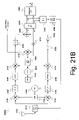
- This method comprises: listening for channel energy on a wireless channel; demodulating the channel energy into a non-synchronized in-phase component and a non-synchronized quadrature phase component; squaring the non-synchronized in-phase component; squaring the non-synchronized quadrature phase component; multiplying the non-synchronized in-phase component and the non-synchronized quadrature phase component to produce an I ⁇ Q product; subtracting the squared non-synchronized quadrature component from the squared non-synchronized in-phase component to produce a first intermediate value; doubling the I ⁇ Q product to produce a second intermediate value; adding the first intermediate value and the second intermediate value to produce a clear channel assessment input value; performing a carrier signal detection function on the clear channel assessment input value to produce a clear channel assessment output value; and using the clear channel assessment output value to determine whether a signal is present in the wireless channel.
- the carrier signal detection function may be a fast Fourier transform function, a decimated fast Fourier transform function, or a band pass filtering function.
- the step of using the clear channel assessment output value to determine whether a signal is present in the wireless channel is preferably performed by determining if the clear channel assessment output value is greater than a set threshold value.
- the step of listening for channel energy may further comprise: performing a variable gain amplification function on the channel energy before the channel energy is demodulated.
- the method of performing a clear channel assessment in a wireless network may further comprise: performing an absolute value function on the clear channel assessment input value to produce a feedback signal.
- the feedback signal is preferably used to control the variable gain amplification function.
- the method of performing a clear channel assessment in a wireless network may further comprise: filtering any frequency components in the non-synchronized in-phase component above a low pass threshold before the step of squaring the non-synchronized in-phase component.
- the method of performing a clear channel assessment in a wireless network may further comprise: filtering any frequency components in the non-synchronized quadrature phase component above a low pass threshold before the step of squaring the non-synchronized quadrature phase component.
- the step of demodulating the channel energy may further comprise: generating a base oscillating signal having a base center frequency; mixing the channel energy with the base oscillating signal to obtain the non-synchronized in-phase component; shifting the base oscillating signal in phase by 90 degrees to obtain a shifted oscillating signal; and mixing the channel energy with the shifted oscillating signal to obtain the non-synchronized quadrature phase component.
- the step of demodulating the channel energy may further comprise: generating a base oscillating signal having a base center frequency; mixing the channel energy with the base oscillating signal to obtain the non-synchronized quadrature phase component; shifting the base oscillating signal in phase by 90 degrees to obtain a shifted oscillating signal; and mixing the channel energy with the shifted oscillating signal to obtain the non-synchronized in-phase component.
- the base center frequency for one band is preferably between 3.1 and 5.1 GHz and more preferably is 4.104 GHz.
- the base center frequency for another one band is preferably between 6 and 10.6 GHz and more preferably is 8.208 GHz.
- a method for performing a clear channel assessment in a wireless network comprises: listening for channel energy on a wireless channel; generating a first base oscillating signal having a base center frequency; generating a second base oscillating signal that is identical to the first base oscillating signals, but shifted in phase by 90 degrees; mixing the channel energy with the first base oscillating signal to obtain a non-synchronized in-phase component; mixing the channel energy with the second base oscillating signal to obtain the non-synchronized quadrature phase component; generating a first corrective oscillating signal having a corrective center frequency; generating a second corrective oscillating signal that is identical to the first corrective oscillating signals, but shifted in phase by 90 degrees; mixing the non-synchronized in-phase component with the first corrective oscillating signal to obtain a corrected non-synchronized in-phase component; mixing the non-synchronized quadrature component with the second corrective oscillating signal to obtain a corrected non-synchronized quadrature component; squaring the corrected non
- the I ⁇ Q product may be used to adjust the corrective center frequency.
- the base center frequency for one band is preferably between 3.1 and 5.1 GHz and more preferably is 4.104 GHz.
- the base center frequency for another one band is preferably between 6 and 10.6 GHz and more preferably is 8.208 GHz.
- the corrective center frequency preferably varies between zero and 100 MHz.
- the carrier signal detection function may be a fast Fourier transform function, a decimated fast Fourier transform function, or a band pass filtering function.
- the step of using the clear channel assessment output value to determine whether a signal is present in the wireless channel is preferably performed by determining if the clear channel assessment output value is greater than a set threshold value.
- the step of listening for channel energy may further comprise: performing a variable gain amplification function on the channel energy before the channel energy is demodulated.
- the method of performing a clear channel assessment in a wireless network may further comprise: performing an absolute value function on the clear channel assessment input value to produce a feedback signal.
- the feedback signal is used to control the variable gain amplification function.
- the method of performing a clear channel assessment in a wireless network may further comprise: filtering any frequency components in the non-synchronized in-phase component above a low pass threshold before the step of mixing the non-synchronized in-phase component with the first corrective oscillating signal.
- the method of performing a clear channel assessment in a wireless network may further comprise: filtering any frequency components in the non-synchronized quadrature phase component above a low pass threshold before the step of mixing the non-synchronized in-phase component with the second corrective oscillating signal.
- FIG. 1 is a graph of a typical UWB pulse stream
- FIG. 2 is a graph showing the power spectral density limits currently put in force by the FCC
- FIGS. 3A-3C are graphs showing exemplary pulse streams for on-off keying, positive pulse amplitude modulation, and binary phase-shift keying, respectively using monopulses, according to a preferred embodiment of the present invention
- FIGS. 4A-4C are constellation diagrams for the modulation schemes of FIGS. 3A-3C , respectively;
- FIGS. 5A-5C are constellation diagrams for pulse position modulation schemes under various conditions for binary pulse position modulation schemes, based on the pulse shown in FIG. 1 ;
- FIGS. 6A-6D are graphs showing component pulses for the decomposition of binary PPM into unmodulated and antipodal pulse trains
- FIG. 7 is a timing diagram showing a one-pulse code word using monopulses according to a preferred embodiment of the present invention.
- FIG. 8 is a timing diagram showing a five-pulse code word using monopulses, according to a preferred embodiment of the present invention.
- FIG. 9A is a graph of an oscillating signal used to form a pulse stream in a preferred embodiment of the present invention.
- FIG. 9B is a graph of an oscillating signal formed in a carrier waveform used to form a pulse stream in a preferred embodiment of the present invention.
- FIG. 9C is a graph of a consecutive series of the oscillating signals of FIG. 9B according to a preferred embodiment of the present invention.
- FIGS. 10A-10C are graphs showing exemplary pulse streams for OOK, PPAM, and BPSK modulation schemes, respectively, using portions of an oscillating signal as pulses, according to preferred embodiments of the present invention
- FIG. 11 is a timing diagram showing a five-pulse code word using a repeated oscillating signal pulse, according to a preferred embodiment of the present invention.
- FIGS. 12A and 12B are timing diagrams showing a five-pulse code word using five ternary pulses, according to preferred embodiments of the present invention.
- FIG. 13 is a graph of a UWB PSD using a notch according to a preferred embodiment of the present invention.
- FIG. 14 is a graph of a UWB transmission scheme using two bands according to a preferred embodiment of the present invention.
- FIG. 15A and 15B are block diagrams of a transmitter and receiver pair according to preferred embodiments of the present invention.
- FIG. 16A is a block diagram of the correlator of FIGS. 15A and 15B having one arm according to a preferred embodiment of the present invention
- FIG. 16B is a block diagram of the correlator of FIGS. 15A and 15B having two arms according to a preferred embodiment of the present invention
- FIG. 16C is a block diagram of the correlator of FIGS. 15A and 15B having more than two arms according to a preferred embodiment of the present invention
- FIGS. 17A and 17B are block diagram showing a UWB system using pseudo-random scrambling, according to preferred embodiments of the present invention.
- FIG. 18 is a block diagram of a data packet according to a preferred embodiment of the present invention.
- FIGS. 19 and 20 are flow charts describing the operation of the transmitter and receiver, respectively, according to a preferred embodiment of the present invention.
- FIGS. 21A and 21B are block diagrams showing circuits for performing a rapid clear channel assessment according to preferred embodiments of the present invention.
- FIG. 21C is a flow chart of a rapid clear channel assessment method according to a preferred embodiment of the present invention.
- FIGS. 22A-22C are block diagrams of a short preamble, a normal preamble, and a long preamble, respectively, according to preferred embodiments of the present invention.
- FIGS. 23A and 23B are graphs showing the output of the squarer elements in FIGS. 21A and 21B for three and seven term squaring, respectively, according to preferred embodiments of the present invention.
- a series of pulses are sent across a transmission medium.
- these UWB pulses need to have data encoded (i.e., modulated) into them.
- a receiver can look at the incoming pulses and decode the original data.
- FIGS. 3A-3C and 6 A- 6 D a number of different approaches have been tried, including various PAM and PPM schemes.
- PPM shifts the position of individual pulses depending upon whether the pulse needs to represent a “1” or a “0.” As shown, for example, in FIG. 6A , in a simple PPM scheme a pulse is moved from a default position by a distance ⁇ T to the left if it represents a “0” and is moved from the default position by a distance ⁇ T to the right if it represents a “1.”
- the pulses don't change, they just advance or delay in time, i.e., the position of these pulses is modulated in time.
- the pulses are generally identical, which makes it easier to generate them.
- FIG. 6A the pulses all rise first and then fall.
- BPSK does not shift the position of the pulses, but rather inverts the pulses to pass data.
- a pulse is unaltered if it represents a “0” and is inverted if it represents a “1.” In either case the position of the pulse remains unchanged.
- BPSK signals will be superior to PPM signals.
- One primary reason is how the two methods handle noise. When a signal gets sent from a transmitter to a receiver, it is subjected to a certain amount of noise. This noise rides on top of the data signal and can distort the signal. Some of the noise comes from going through the channel (i.e., the transmission medium). Additional noise comes from the receiver, which has to amplify a very small signal. Such an amplification process inherently introduces noise.
- the way to compare individual transmission schemes is to determine the maximum amount of noise allowable before the system exceeds a maximum error rate, In any transmission system some errors will occur, due to noise and other reasons. A given system will set a maximum allowable error rate, which it is designed to compensate for. Beyond this error rate, the system will not achieve a desired level of performance.
- An exemplary maximum error rate often called a bit error rate (BER) is one error in a thousand, often described as having a BER of 10 ⁇ 3 .
- a PPM signal will require twice as much transmit power to achieve the same BER as a BPSK signal.
- the BPSK signal is superior to the PPM signal by 3 dB (i.e., by a factor of two in power).
- the BPSK signal will tolerate more noise than a PPM signal.
- the PPM signal would require more power than the BPSK signal.
- PAM pulse amplitude modulation
- M-ary Such alternative transmission schemes may be called M-ary systems.
- M-ary simply means that there are M different choices for encoding data.
- Alternate systems could have M equal to four (4-ary), M equal to eight (8-ary), or any other acceptable number. Powers of two are preferable for M since it makes implementation easier, but are not required.
- each pulse has M different ways that it can be sent to the receiver.
- an M-ary PAM system (called an MPAM system) would have M different pulse voltages that can be used.
- M-PAM multipath-induced inter-symbol interference
- the binary PPM technique can also be extended to M-ary orthogonal (or non-orthogonal) PPM by mapping b bits to a single pulse (or pulse train) and using 2 b different values for the pulse position.
- M-ary orthogonal signaling will provide better distance properties for higher dimensions, resulting in better power efficiency relative to binary PPM.
- M-ary PPM can be analyzed by extending the decomposition techniques describe earlier for the binary case. It is known that M-ary orthogonal constellation do have non-zero means and this technique would therefore still result in spectral lines and suboptimal power efficiency.
- M-ary bi-orthogonal keying involves the mapping of b bits to a group of consecutive bi-phase pulses.
- MBOK provides improved power efficiency relative to binary antipodal signaling, yet would still not generate spectral lines for white data.
- M-PAM M 2 voltages
- 8-PAM 4-PAM
- M-PAM is generally limited to cases where M>2, since a 2-PAM system would be equivalent to a basic BPSK system.
- UWB systems preferably transmit at extremely small power levels, but at very wide bandwidths. Thus, although they generally have essentially as much bandwidth as they want, UWB systems must maintain very low power levels to be efficient. Therefore, it's desirable to choose a modulation scheme that is extremely power efficient.
- M-PAM modulation is less power efficient than BPSK modulation, for example, consider an 8-PAM transmission scheme. Although it appears that such a scheme would be more efficient (after all, it's transmitting three times as much data in a similar transmission using BPSK), it turns out to be less power efficient than BPSK. The reason for this is that an M-PAM modulation scheme requires much higher power levels for many of its pulses.
- the system need only send a single 1 ns pulse every 10 ns—a reasonable requirement. This can potentially allow for more pulses to be sent, thus increasing the rate of data transmission. However, this is limited by the size of the pulse and the minimum allowable distance between pulses. Once the pulses are so close that they are only that minimum distance from each other, the system can no longer increase the pulse transmission rate without having pulses collide.
- An alternative to sending data as individual pulses is to instead represent each bit by a series of pulses.
- This series of pulses can be called a code word.
- a set of BPSK pulses will preferably be chosen to represent a “0” and its inverse will preferably be chosen to represent a “1.”
- code words Individual pulses are then ordered together into code words to transfer data at a given data rate, with each code word corresponding to one or more bits of information to be transferred.
- the code words have a code word period T cw , indicating the duration of an code word, and a related code word frequency F cw . This may correspond to the data rate, though it does not have to.
- FIGS. 7 and 8 show two examples of code words.
- FIG. 7 is a timing diagram showing a one-pulse code word using monopulses according to a preferred embodiment of the present invention.
- This simplest example has a code word that includes a single pulse.
- the code word period T cw and the pulse period T p are the same (i.e., the pulses and the code words are transmitted at the same frequency).
- the non-inverted pulse corresponds to a “1,” and the inverted pulse corresponds to a “0.” This could be reversed for alternate embodiments.
- FIG. 8 is a timing diagram showing a five-pulse code word using monopulses according to a preferred embodiment of the present invention.
- This embodiment has a code word that includes five binary pulses.
- the code word period T cw is five times the pulse period T p (i.e., the code words are transmitted at one-fifth the frequency of the pulses).
- the pulse period T p and number of pulses n per code word determine the period of the code word T cw .
- a particular orientation of the five pulses corresponds to a “1,” and the inverse of this orientation corresponds to a “0.”
- the particular choice of pulse orientation and arrangement within the code word is not critical, and can be varied as necessary. What is important is that the “1” and “0” code words are the inverse of each other.
- One preferred embodiment includes 13 analog pulses per code word, and sets the pulse frequency F p at 1.3 GHz (770 ps pulse period T p ). This results in a code word frequency F cw of 100 MHz (10 ns code word period T cw ), which corresponds to a data transfer rate of 100 Mbits of information per second.
- Another preferred embodiment includes 24 analog pulses per code word, and sets the pulse frequency F p at either 1.368 GHz or 2.736 GHz (731 ps or 365.5 ps pulse period T p ) for each of two bands used.
- the various parameters of peak-to-peak pulse width T p-p , pulse period T p , pulse frequency F p , number of pulses per code word n, code word period T cw , and code word frequency F cw can be varied as necessary to achieve the desired performance characteristics for the transceiver.
- the embodiments disclosed in FIGS. 7 and 8 have the same code word period T cw , despite the differing number of pulses n. This means that the transmission power for a given code word period T cw is used in a single pulse in the embodiment of FIG. 7 , but is spread out over five pulses in the embodiment of FIG. 8 . Alternate embodiments can obviously change these parameters as needed.
- the transmitter when a transmitter passes a bit of data to a receiver, the transmitter sends the bit as a code word (i.e., a set series of pulses).
- the bits are preferably represented by inverse code words such that the non-inverted code word represents a “1” and the inverted code word represents a “1.”
- this assignment of code word/inverse code word to “1” and “0” values can be reversed.
- FIG. 8 shows a code word having five pulses for the sake of simplicity, this number can be varied as needed. In fact, as noted above, 13 or 24 are preferred numbers of pulses per code word. Alternate embodiments can use any code word length that allows system requirements to be met. For example, as clock speeds increase, the number of pulses that can be sent in a given time will increase and longer code word lengths may be used.
- One advantage with using a code word is that you can spread out a required transmission power over multiple pulses. For a successful transmission, it's necessary to use a certain amount of energy to send each bit. If the bit is sent in a single pulse, that pulse has to include all of the required energy. This requires a larger pulse and increases the peak-to-average ratio of the signal (i.e., the entire waveform). However, if five pulses are used to send a single bit of data (as shown in the embodiment of FIG. 8 ), the energy can be spread out among five separate pulses. Thus, each individual pulse can be smaller and can have a lower peak-to-average ratio.
- UWB signals must fall below a set power maximum for any given frequency. In other words, the energy of the UWB signal cannot exceed the set power maximum at any frequency. Therefore, it is necessary that the UWB signal fit within the power spectrum density requirements set forth in FIG. 2 .
- the amount of energy sent in a transmission is equal to the area under its power spectrum density curve. For the best possible system performance, it's preferable that this area be maximized. In other words, it is desirable to have a signal whose properties fits under the restricted curve, but is arranged to have a maximum possible area.
- the power spectrum density ends up looking wavy, with numerous peaks and valleys. The exact waviness of the power spectrum density depends upon the particular sequence of pulses used.
- the peaks in the PSD curve can limit the transmission power by limiting the maximum total power transmitted. Since the power spectrum density cannot ever go above the power maximum set by the FCC, the maximum point of the power spectrum density curve can be no higher than the allowable power maximum. If there are too many peaks (and corresponding valleys) in the power spectrum density curve (or even just one big one), the overall area under the power spectrum density curve can be significantly reduced by the presence of one or more large valleys, indicating a lower overall transmission power for the UWB signal. Thus, a smoother power spectrum density curve is preferable because that maximizes the area under the curve.
- pulses are short duration pulses formed using a single basic pulse shape (e.g., a monopulse), with the interval between individual pulses being uniform or variable.
- pulses can be formed in different ways.
- portions of an oscillating carrier signal are used as pulses, e.g., three repetitions of the oscillating signal. These portions of the oscillating signal could be treated just as the pulses in FIG. 1 , i.e., adjusted in amplitude or phase as shown in FIGS. 3A-3C .
- An example of a typical oscillating signal used to form a pulse stream in a preferred embodiment of the present invention is shown in FIG. 9A .
- these sorts of signals are used in a BPSK system, they can be referred to as n-cycle BPSK (e.g., the preferred embodiment of FIG. 9A is a three-cycle BPSK signal that uses three repetitions of a base oscillating signal).
- the carrier frequency of the oscillating signal (i.e., 1/T p-p ) in this embodiment is three times the chipping rate.
- the frequency of the waveform of the oscillating signal is three times the frequency of the pulses used by the network. This allows the network to take advantage of second order statistics that are unique to BPSK systems, and will allow improved acquisition.
- UWB using monopulses can be called a carrier-less radio system
- a carrier-based system in which segments of the carrier are used to form pulses.
- an oscillating signal could be further modulated by a carrier signal having a lower frequency (e.g., 1/N).
- the carrier could serve to modulate a set of N repetitions of the oscillating signal. These N repetitions of the oscillating signal (modulated by the carrier) form a pulse. This is similar to the embodiment of FIG. 9A , with the addition of the carrier signal.
- FIG. 9B is a graph of an oscillating signal formed in a carrier waveform used to form a pulse stream in a preferred embodiment of the present invention. As shown in FIG. 9B , N is chosen to be three. In other words, three repetitions of the oscillating signal (modulated by the carrier) form a pulse.
- FIG. 9C is a graph of a consecutive series of the oscillating signals of FIG. 9B according to a preferred embodiment of the present invention. This graph shows how the modulated pulses of this embodiment flow together in a stream to pass data.
- FIGS. 10A-10C are graphs showing exemplary pulse streams for OOK, PPAM, and BPSK modulation schemes, respectively, using portions of an oscillating signal as pulses. In each case, they show a data sequence “1 0 1 0.”
- OOK defines the data by the presence or absence of a pulse.
- a “1” is indicated by a pulse, and a “0” is indicated by the absence of a pulse.
- the bit stream “1 0 1 0” is indicated by the sequence of: a pulse, a blank where a pulse should be, a pulse, and another blank.
- PPAM defines the data by the amplitude of the pulse.
- a “1” is indicated by a large pulse, and a “0” is indicated by a small pulse.
- the bit stream “1 0 1 0” is indicated by the sequence of: a large pulse, a small pulse, a large pulse, and a small pulse.
- This embodiment uses strictly positive values for the two pulse weights, so that a k ⁇ 0 , ⁇ 1 ⁇ where 0 ⁇ 0 ⁇ 1 .
- BPSK defines the data by the polarity of the pulse.
- a “1” is indicated by a non-inverted pulse
- a “0” is indicated by an inverted pulse.
- the bit stream “1 0 1 0” is indicated by the sequence of: a non-inverted pulse, an inverted pulse, a non-inverted pulse, and an inverted pulse.
- a k ⁇ 1,+1 ⁇ This corresponds to transmitting either a non-inverted or an inverted pulse based on the value of the source bit.
- FIG. 11 is a timing diagram showing a five-pulse code word using repeated oscillating signal pulses, according to a preferred embodiment of the present invention.
- This embodiment has a code word that includes five binary pulses.
- the code word period T cw is five times the pulse period T p (i.e., the code words are transmitted at one-fifth the frequency of the pulses).
- the pulse period T p and number of pulses n per code word determine the period of the code word T cw .
- a particular orientation of the five pulses corresponds to a “1,” and the inverse of this orientation corresponds to a “0.”
- the particular choice of pulse orientation and arrangement within the code word is not critical, and can be varied as necessary. What is important is that the “1” and “0” code words are the inverse of each other.
- the oscillating signal is a Gaussian monopulse with a peak-to-peak time (T p-p ) of a fraction of a nanosecond, a pulse period T p of several nanoseconds, and a bandwidth of several gigahertz.
- T p-p and T p can be used for different values. And in embodiments in which more or fewer repetitions are used to designate a pulse, the relationship between T p-p and T p can also vary.
- the embodiments above show the use of binary values (i.e., 1 and ⁇ 1) for creating code words, it is also possible to use ternary values (i.e., 1, 0, ⁇ 1) to create the code words in alternate preferred embodiments.
- the code word will be made up not just of a series of non-inverted and inverted pulses, but rather a series of non-inverted pulses, inverted pulses, and zeroed pulses.
- the zeroed pulses are preferably the absence of either a non-inverted pulse or an inverted pulse.
- FIGS. 12A and 12B are timing diagrams showing a five-pulse code word using five ternary pulses, according to preferred embodiments of the present invention.
- FIG. 12A shows an embodiment using waveforms made of monopulses.
- FIG. 12B shows an embodiment using portions of a continuous oscillating waveform as pulses.
- the code word period T cw is five times the pulse period T p (i.e., the code words are transmitted at one-fifth the frequency of the pulses).
- the pulse period T p and number of pulses n per code word determine the period of the code word T cw .
- a particular orientation of the five pulses corresponds to a bit value of “1,” and the inverse of this orientation corresponds to a bit value of “0.”
- the particular choice of pulse orientation and arrangement within the code word is not critical, and can be varied as necessary. What is important is that the “1” and “0” code words are the inverse of each other.
- each ternary pulse can have a value of 1, 0, or ⁇ 1.
- a “1” inverts to a “ ⁇ 1”
- a “ ⁇ 1” inverts to a “1”
- a “0” remains a “0.”
- the code word is defined by the five consecutive pulse values of 1 0 1 ⁇ 1 ⁇ 1, and the inverse code word is defined by the five consecutive pulse values of ⁇ 1 0 ⁇ 1 1 1.
- these values are imposed on monopulses.
- these values are imposed on segments of a continuous oscillating waveform.
- pulse values are ternary rather than binary, they operate just as the code words described above with respect to FIGS. 7 , 8 , and 11 .
- FIGS. 12A and 12B each show a code word having five pulses, this number can be varied as needed. Alternate embodiments can use any code word length that allows system requirements to be met. For example, as clock speeds increase, the number of pulses that can be sent in a given time will increase and longer code word lengths may be used. In three preferred embodiments these code words are 12, 13, and 24 ternary pulses in length.
- the FCC will freely allow transmissions that do not violate the power spectral density (PSD) limitations shown in FIG. 2
- PSD power spectral density
- UNII National Information Infrastructure
- the UNII band is used by such devices as IEEE 802.11a devices, cordless telephones, HiperLAN2 devices, etc.
- a UWB system can both reduce the chance that it will interfere with devices that use the UNII band, and the chance that those devices will interfere with transmissions by the UWB system.
- FIG. 13 is a graph of a UWB PSD using a notch according to a preferred embodiment of the present invention.
- the notch is placed within the UNII band such that the UWB signal's spectrum falls on either side of the UNII band.
- This can be achieved by having a UWB system, whose carrier frequency is centered in the UNII band, and which has a notch at the carrier frequency. In this way, an RF spectral notch will fall right in the UNII band.
- the notch is placed at a frequency slightly lower than the center of the UNII band to give maximum protection to the lower and central portions of the UNII band. This is because most of the UNII band devices operate in the lower or central portions of the band.
- the upper range of the UNII band is primarily used for outdoor point-to-point links.
- UWB signals across a large spectrum can be formed as a single band, they can also be formed in two or more bands. These separate bands each have a different power spectral density, and would be limited to a subset of the total available bandwidth.
- the power spectral density (PSD) for the UWB system can be more easily manipulated. For example, certain portions of the available bandwidth can be avoided, or simply used with different PSD parameters than other portions.
- Each different overlapping device could then use a separate band. Although the transmissions of the overlapping devices would be sent within the same physical area, the interference each would experience with respect to each other would be limited by the separation of the two bands.
- FIG. 14 is a graph of a UWB transmission scheme using two bands according to a preferred embodiment of the present invention.
- the high band has a center frequency of 8.208 GHz with a 3 dB bandwidth of 2.736 GHz
- the low band has a center frequency of 4.104 GHz with a 3 dB bandwidth of 1.368 GHz.
- the high band in FIG. 14 preferably uses pulses that are made up of three iterations of an oscillating signal (e.g., a signal from a sine wave generator) having a frequency of 8.208 GHz (which can be called the high carrier frequency).
- the low band preferably uses pulses that are made up of three iterations of an oscillating signal (e.g., a signal from a sine wave generator) having a frequency of 4.104 GHz (which can be called the low carrier frequency).
- the UWB system is set such that both the low band has a ⁇ 3 dB point at 4.788 GHz, and the high band has a ⁇ 3 dB point at 6.840 GHz. This gives a gap of 2.052 GHz between the two ⁇ 3 dB points, just about in the middle of the UNII band. In this way, interference is minimized between the UWB transmissions and any transmissions being made by other devices in the UNII band.
- the UWB transmission system shown in FIG. 14 limits its interference with any other signals being transmitted in the UNII band, while also providing two separate transmission paths.
- UWB included one constant pressure in any transmission scheme, UWB included, is the desire to scale the transmission rate upward, (i.e., send more data bits faster). For example, instead of sending a hundred megabits, we want to send hundreds of megabits.
- the data rate can be sped up.
- One way is to send more pulses through within the same period of time. This would involve either reducing the width of the individual pulses or reducing the spacing between adjacent pulses.
- Another way is to use a smaller code word. As you drop pulses off of the code word, the code word takes less time to transmit and thus allows more to be sent in a given time.
- Yet another alternative is to use multiple code words to represent more than just a binary bit of data. Rather than just using a code word and its inverse, you could use multiple different code words, each representing a different combination of multiple bits. For example, if the code word is five pulses long, there are thirty-two different ways that inverted and non-inverted pulses can be combined to form a code word. Counting for the fact that half of these will be the inverse of others, this allows for sixteen possible code words. This potentially allows up to five bits of data to be sent in the time it takes for five pulses to be sent. The receiver can determine which bits of data have been sent by determining which combination of inverted and non-inverted pulses have been received as the code word.
- this system allows for log 2 (C) bits to be sent, where C is the number of code words used.
- C is the number of code words used.
- log 2 (32), or 5 bits could be sent.
- FIGS. 15A and 15B are block diagrams of transmitter and receiver pairs according to preferred embodiments of the present invention.
- the transmitter and receiver pair 1500 a in FIG. 15A is used to produce binary code words.
- the transmitter and receiver pair 1500 b in FIG. 15B is used to produce ternary code words.
- the transmitter receiver pair 1500 a includes a transmitter 1510 a and a receiver 1520 .
- the transmitter 1510 includes a lookup table 1530 , a pulse forming network (PFN) 1535 a , an adder 1540 , and a transmitting antenna 1545 .
- the receiver 1520 includes a receiving antenna 1550 , a front end 1555 , and a correlator 1560 .
- the transmitter receiver pair 1500 b includes a transmitter 1510 b and a receiver 1520 .
- the transmitter 1510 includes a lookup table 1530 , a pulse forming network (PFN) 1535 b , an adder 1540 , and a transmitting antenna 1545 .
- PPN pulse forming network
- the receiver 1520 includes a receiving antenna 1550 , a front end 1555 , and a correlator 1560 . These two operate in the same manner except for the operation of the PFN 1535 a , 1535 b in each transmitter 1510 a , 1510 b.
- the lookup table 1530 receives a bit stream, breaks the bit stream up into n-bit groups, and determines the proper code word associated with that particular n-bit group. It then sequentially outputs a series of “1”s and “0”s corresponding to the proper code word.
- n can be any integer greater than 0.
- the PFN 1535 a receives the string of “1”s and “0”s that define the code word from the lookup table 1530 and outputs either a non-inverted or an inverted pulse in response to each input value.
- the PFN 1535 a receives a clock signal CLK and a code word as inputs, and has non-inverted and inverted outputs. Whenever the clock CLK cycles, the PFN 1535 outputs either a non-inverted pulse at the non-inverted output, or an inverted pulse at the inverted output, depending upon the value of the individual portions of the code word.
- the PFN 1535 b receives the string of “1”s, “0”s, and “ ⁇ 1”s that define the code word from the lookup table 1530 and outputs either a non-inverted pulse, a zeroed pulse, or an inverted pulse in response to each input value.
- the PFN 1535 b receives a clock signal CLK and a code word as inputs, and has non-inverted, zeroed, and inverted outputs.
- the PFN 1535 Whenever the clock CLK cycles, the PFN 1535 outputs either a non-inverted pulse at the non-inverted output, a zeroed pulse at the zeroed output, or an inverted pulse at the inverted output, depending upon the value of the individual portions of the code word.
- the pulses output from the PFN 1535 a , 1535 b can be any variety of pulses.
- the pulses are individual monopulses.
- the pulses are sections from an oscillating signal. Alternate embodiments could use other pulses, if desired, however.
- the adder 1540 then adds together the inverting and non-inverting outputs (and zeroed output, if any), only one of which should be active at a time, to provide a single output pulse.
- this output pulse will be either a positive (non-inverting) pulse or a negative (inverted) pulse, depending upon the value of the current portion of the code word when the clock CLK cycles.
- this output pulse will be either a positive (non-inverting) pulse, a zeroed pulse, or a negative (inverted) pulse, depending upon the value of the current portion of the code word when the clock CLK cycles.
- Alternate embodiments of the PFN 1535 could have a single output that outputs either a non-inverted or inverted pulse (or a non-inverted, zeroed, or inverted pulse) depending upon the value of the current portion of the code word. In such embodiments there is no need for the adder 1540 .
- the output of the adder 1540 is then sent to the transmitting antenna 1545 , which transmits the pulses to the receiver 1520 .
- the receiving antenna 1550 receives the pulses in a signal sent by the transmitting antenna 1545 in the transmitter 1510 .
- the front end 1555 preferably performs necessary operations on the received signal to better allow the remainder of the receiver 1520 to properly process it. This can include performing filtering and amplifying the signal.
- the correlator 1560 receives a code word from the front end, determine what n-bit group corresponds to that code word (or inverse code word) and outputs the corresponding n-bit group.
- the correlator 1560 will have to have as many different branches (called arms or fingers) to look for code words as there are individual code words.
- a single code word can be used to send a bit stream from the transmitter 1510 to the receiver 1520 one bit of data at a time.
- the transmitter 1510 takes the bit stream, separates the stream into individual bits, chooses a code word/code word inverse based on the bit to be transmitted, and then sends the chosen code word/inverse to the receiver 1520 .
- the correlator 1560 in the receiver 1520 then needs to check each incoming n-bits to see if they correspond to the code word or its inverse. Since the correlator 1560 needs to look for only one code word, it needs only one arm (i.e., only one set of circuitry devoted to correlating a code word).
- FIG. 16A is a block diagram of the correlator of FIGS. 15A and 15B having one arm according to a preferred embodiment of the present invention.
- the correlator 1560 includes a mixer 1610 , an integrator 1615 , and a decision circuit 1620 .
- the mixer 1610 receives the incoming signal and the code word. It mixes the code word CW and a portion of the incoming signal equal in length to the code word and outputs the result to the integrator 1615 .
- the integrator 1615 integrates the output of the mixer 1610 over the length of the code word to produce a correlation result.
- This correlation result will be a large number if the code word is matched or a large negative number if the inverse of the code word is matched.
- the decision circuit 1620 determines what data bit the code word corresponds to (i.e., a “1” or a “0”), and outputs that data bit to other circuitry in the receiver 1520 .
- the single input stage (i.e., the mixer 1610 ) on the correlator 1560 corresponds to the correlators 1560 one arm.
- multiple code words can be used to send multiple bits at the same time. For example, to send two data bits at a time, two different code words should be used. Each code word then represents two bits of data. In this case, if the bit stream to be transmitted were 0111001101001001, the transmitter would break it up into two bit sections as so: (01)(11)(00)(11)(01)(00)(10)(01).
- the transmitter 1510 takes the bit stream to be sent to the receiver 1520 , separates the stream into 2-bit sections, chooses a code word/code word inverse based on the two bits to be sent, and sends the chosen code word/inverse to the receiver 1520 .
- the correlator 1560 in the receiver 1520 then needs to check each incoming n-bits to see if they correspond to the first or second code word or their inverses. Since the correlator 1560 needs to look for two code words, it needs two arms (i.e., two sets of circuitry devoted to correlating a code word).
- FIG. 16B is a block diagram of the correlator of FIGS. 15A and 15B having two arms according to a preferred embodiment of the present invention.
- the correlator 1560 includes first and second mixers 1610 1 and 1610 2 , first and second integrators 1615 1 and 1615 2 , and a decision circuit 1620 .
- the mixers 1610 1 and 1610 2 each receive the incoming signal and one of the two code words CW 1 or CW 2 .
- Each mixer 1610 1 , 1610 2 mixes the respective code word and a portion of the incoming signal equal in length to the code words and outputs the result to the first and second integrators 1615 1 and 1615 2 , respectively.
- the first and second integrators 1615 1 and 1615 2 integrate the output of each of the mixers 1610 1 and 1610 2 over the length of the code word to produce first and second correlation results, respectively.
- Each correlation result will be a large number if the code word is matched, a large negative number if the inverse of the code word is matched, or a lower value if neither the code word nor its inverse is matched.
- the decision circuit 1620 determines what two data bits the code word corresponds to (i.e., “00,” “01,” “10,” or “11”), and outputs those two data bits to other circuitry in the receiver 1520 .
- This examination can be performed, for example, by setting a threshold for correlation values, above which a correlation is considered successful, by comparing all of the correlation values and picking the largest result as a successful correlation, or a combination of the two.
- the double input stage (i.e., mixers 1610 1 and 1610 2 ) on the correlator 1560 corresponds to the two arms of the correlator 1560 .
- the transmitter 1510 takes the bit stream to be sent to the receiver 1520 , separates the stream into n-bit sections (where n is greater than 2), chooses a code word/code word inverse based on the n bits to be sent, and sends the chosen code word/inverse to the receiver 1520 .
- the correlator 1560 in the receiver 1520 then needs to check each incoming n-bits to see which of the first through k th code words (or inverses) they correspond to. Since the correlator 1560 needs to look for k code words, it needs k arms (i.e., k sets of circuitry devoted to correlating a code word).
- FIG. 16C is a block diagram of the correlator of FIGS. 15A and 15B having more than two arms according to a preferred embodiment of the present invention.
- the correlator 1560 includes first through k th mixers 1610 1 to 1610 k , first through k th integrators 1615 1 to 1615 k , and a decision circuit 1620 .
- the mixers 1610 1 to 1610 k each receive the incoming signal and one of the k code words CW 1 to CW k .
- Each mixer 1610 1 , . . . , 1610 k mixes the respective code word and a portion of the incoming signal equal in length to the code words and outputs the result to the first through k th integrators 1615 1 to 1615 k , respectively.
- the first through k th integrators 1615 1 and 1615 k integrate the output of each of the mixers 1610 1 to 1610 k over the length of the code word to produce first through k th correlation results, respectively.
- Each correlation result will be a large number if the respective code word is matched, a large negative number if the inverse of the respective code word is matched, or a lower value if neither the respective code word nor its inverse is matched.
- the decision circuit 1620 determines what b data bits the code word corresponds to, and outputs those b data bits to other circuitry in the receiver 1520 .
- This examination can be performed, for example, by setting a threshold for correlation values, above which a correlation is considered successful, by comparing all of the correlation values and picking the largest result as a successful correlation, or a combination of the two.
- the multiple input stage (i.e., mixers 1610 1 through 1610 k ) on the correlator 1560 corresponds to the k arms of the correlator 1560 .
- the correlator 1560 preferably looks for the code words rather than individual pulses. If the correlator 1560 looked for each individual pulse, it would have to make a lot more decisions, since it would check a larger number of individual pulses. The complexity of the system can be significantly reduced by having the correlator 1560 look instead for a long sequence of pulses.
- the correlator 1560 has multiple arms (i.e., multiple mixers 1610 1 to 1610 k ).
- the decision circuit 1620 has to take the first through k th correlation results from these mixers 1610 1 to 1610 k and compare them to determine which code word (or inverse) was received. By choosing code words that are orthogonal to each other, the function performed by the decision circuit 1620 can be greatly simplified.
- the i th mixer 1610 i when a particular code word (or its inverse) sent from the transmitter 1510 is received by the i th mixer 1610 i and is mixed with the respective code word CW i , the i th mixer 1610 i will output a large positive number if the received code word matches the i th code word, and will output a large negative number if the received code word matches the inverse of the i th code word.
- the i th mixer will output a non-zero value somewhere between the large negative number and the large positive number. However, if the code words are orthogonal to each other, then if the received code word does not match the i th code word CW i , the i th mixer will output a value of zero.
- One way the decision circuit 1620 can decide which correlation value is the correct one (i.e., which indicates the proper code word) is that it examines all of the outputs of the receiver mixers 1610 1 to 1610 k and looks for the one that has the largest absolute value. Ideally, the other receiver multipliers should have an output close to zero.
- the decision circuit 1620 looks at the sign of the chosen correlation value. If it is positive, then the non-inverted code word has been received; if it is negative, then the inverted code word has been received.
- the system allows the receiver to make a much easier comparison of correlation values, since when the code words are orthogonal, one correlation value will be a large positive or negative number (i.e., the one corresponding the received code word), and all of the other correlation values will be zero (or close to zero, accounting for the presence of noise in the system). Thus, when the absolute value of the output of the correlator corresponding to the received code word is at a maximum, the output of the other correlators will be zero.
- orthogonal code sets are not difficult to find. For example, if you have a code word of twelve pulses, (i.e., a length twelve code word), you would have 2 12 or 4096 possible code words. From this set of 4096 possible code words there is at lease one set of twelve codes that are mutually orthogonal, as shown in Table 3. Other orthogonal subsets also exist.
- Tables 4A-4D show examples of sets of orthogonal 24-bit code words for up to four overlapping networks.
- Table 4A shows the code words used for the first network;
- Table 4B shows the code words used for the second network;
- Table 4C shows the code words used for the third network; and
- Table 4D shows the code words used for the fourth network.
- Code sets that are nearly orthogonal refers to code word sets in which the correlation between different code words from the set gives results that are greater than zero, but are smaller than an acceptable threshold.
- This threshold can be determined based on the ability of the correlator to differentiate between a correct code word correlation and an incorrect code word correlation.
- One possible threshold is a random correlation threshold, which corresponds to the expected correlation value that random noise would give.
- a set of codes would be considered nearly orthogonal if the correlation between all combinations of different code words in the set give results that are better than the expected correlation between any of the code words and a set of random bits equal in length to the code word.
- alternate embodiments could use a different threshold.
- 2-BOK, 4-BOK, and 8-BOK implementations are used with length 24 codes, and a 64-BOK implementation is used with a length 32 code.
- One added advantage of using more than one arm in the correlator 1560 is that other functions of the receiver 1520 , 1720 can also make use of these features, For example, during signal acquisition, multiple arms can be used not to look for multiple code words, but to find a single code more quickly, speeding up the acquisition process. Likewise, in a cluttered environment where a signal bounces off walls or other obstructions and as a result the receiver 1520 , 1720 receives multiple copies of the same signal (often referred to as multipath), the multiple arms can track different time-displaced versions of the same signal to determine which provides the strongest signal. By tracking the same code with two different arms, the receiver 1520 , 1720 can get better performance.
- the multiple arms in the correlator can be used for fast acquisition, multipath reception, or multiple code words.
- the multiple arms are used to speed up acquisition. If, after the signal is acquired, the signal quality is low due to the multipath effect, the multiple arms can then be used to track different time-shifted versions of the same signal. If, however, signal quality is good, then the multiple arms can be used to accommodate multiple code words and thereby speed up data transmission.
- the multiple arm structure is configurable into a variety of uses that can improve system speed or performance. And if none of these uses are required, the additional arms of the correlator can be turned off to save power.
- ADCs analog-to-digital converters
- the decision circuit 1620 in the correlator 1560 receives an analog correlation signal from each mixer 1610 i , and outputs a digital data signal to another portion of the receiver 1520 , it will have to have at least one ADC to convert the received analog signal to a digital signal.
- the ADC in the decision circuit 1620 would need to operate at the full data transmission speed. For example, if the receiver 1520 was operating at 400 MBPS, the ADC would also have to operate at 400 MBPS—making 400 million decisions every second.
- the receiver 1520 used four arms in its correlator 1560 (i.e., four mixers 1610 1 to 1610 4 to check for four separate code words CW 1 to CW 4 at the same time), then it would require four ADCs in the decision circuit 1620 , each operating at 100 MBPS—making only 100 million decisions every second. This makes for a simpler design, since it is easier to design lower speed ADCs. As the speed of ADCs increase they have to have a higher performance, be of higher quality, have less distortion, etc. than a lower speed ADC. This is usually more expensive, may take up more chip area, and may require a more expensive processing technology to create than a larger number of slower ADCs. Generally it is better to use multiple slow ADCs than one fast one.
- the concept of multiple code words is scalable, with the only limit being the number of correlators required in the receivers. If you want to send b bits at a time, then you need 2 (b ⁇ 1) code words and therefore 2 (b ⁇ 1) arms in the correlators 1560 of each receiver 1520 .
- the number of bits b sent at a time is preferably between 2 and 5, i.e., 4 to 16 arms in each correlator 1560 .
- the number of workable correlators in a receiver will expand and the number of usable codes will similarly increase.
- M-ary bi-orthogonal keying MBOK
- MBOK M-ary bi-orthogonal keying
- a transmission will suffer fewer errors for the same amount of noise that's present in the system as compared to BPSK or PPM.
- a coding gain i.e., a more power efficient modulation scheme.
- the transmitter 1510 would use less transmission power. Equivalently for the same amount of transmission power, the receiver 1520 would suffer fewer errors.
- the transmitter 1510 can either transmit at a lower power to achieve that BER, or the signal could be sent over a longer distance before it reached its maximum BER because of the increased power efficiency. In other words, the system is more robust to errors allowing better range and better performance.
- the FCC has limited the power spectral density (PSD) of UWB signals.
- PSD power spectral density
- One way to smooth out the PSD in a code word implementation is to use very long code words. The longer the code words, the more they will look like random transmissions, and the smoother the PSD curve. However, if the code words are made longer than they need to be, available transmission time will be wasted, reducing the maximum data rate allowed by the system.
- the pseudo-random sequence is a sequence of +1 and ⁇ 1 values that is predictable and preferably longer than a code word, but looks random (i.e., has no discernable pattern).
- the pseudo-random sequence should be either known to both transmitter and receiver, or there should be a deterministic way of producing this pattern, e.g., performing a function that starts from a known sequence, that is known by both the transmitter and the receiver.
- both the transmitter and the receiver will be able to produce the pseudo-random sequence and the scrambling can be both performed and undone. This will make the scrambling completely transparent to the rest of the system.
- the transmitter will take a string of code words (or inverses) and scramble them into a pseudo random pattern. This will flatten out the spectrum of the transmitted signal, reducing the number of sharp peaks in its PSD. This eliminates the need to worry about the spectrum properties of the chosen code words, since the pseudo-random scrambling eliminates any short-term regularity in those codes, essentially whitening the transmission. Then the receiver reverses the process and obtains the encoded data.
- pseudo-random scrambling enables the system use the advantageous properties of bi-orthogonal keying, but with superior power efficiency.
- FIGS. 17A and 17B are block diagrams of transmitter and receiver pairs using pseudo-random scrambling according to preferred embodiments of the present invention.
- the transmitter and receiver pair 1700 a in FIG. 17A is used to produce binary code words.
- the transmitter and receiver pair 1700 b in FIG. 17B is used to produce ternary code words.
- the transmitter receiver pair 1700 a includes a transmitter 1710 a and a receiver 1720 .
- the transmitter 1710 a includes a lookup table 1530 , a pulse forming network (PFN) 1535 a , an adder 1540 , a transmitting antenna 1545 , a transmitter mixer 1770 , a transmitter pseudo-random sequence generator 1775 , and a transmitter switch 1778 .
- the receiver 1720 includes a receiving antenna 1550 , a front end 1555 , a correlator 1560 , a receiver mixer 1780 , a receiver pseudo-random sequence generator 1785 , a receiver switch 1788 , and an acquisition circuit 1790 . As shown in FIG.
- the transmitter receiver pair 1700 b includes a transmitter 1710 b and a receiver 1720 .
- the transmitter 1710 b includes a lookup table 1530 , a pulse forming network (PFN) 1535 b , an adder 1540 , a transmitting antenna 1545 , a transmitter mixer 1770 , a transmitter pseudo-random sequence generator 1775 , and a transmitter switch 1778 .
- the receiver 1720 includes a receiving antenna 1550 , a front end 1555 , a correlator 1560 , a receiver mixer 1780 , a receiver pseudo-random sequence generator 1785 , a receiver switch 1788 , and an acquisition circuit 1790 . These two operate in the same manner except for the operation of the PFN 1535 a , 1535 b in each transmitter 1710 a , 1710 b.
- FIGS. 17A and 17B that are the same as FIGS. 15A and 15B operate in the same or similar manner and so their description will not be repeated.
- the transmitter pseudo-random sequence generator 1775 operates to generate a long pseudo-random sequence.
- the transmitter pseudo-random sequence generator 1775 is a shift register that has the pseudo-random sequence entered into it. More specifically, in the preferred embodiment the transmitter pseudo-random sequence generator 1775 is a liner feedback shift register.
- the transmitter pseudo-random sequence generator 1775 has a number of storage locations that contain the long, pseudo-random sequence (i.e., a long string of pseudo-random +1 and ⁇ 1 values). In a preferred embodiment the transmitter pseudo-random sequence generator 1775 contains between fifteen and thirty entries, though it may have more or fewer in alternate embodiments.
- the pseudo-random sequence is shifted through the pseudo-random sequence generator 1775 each time the lookup table 1530 outputs a pulse, and the top entry is multiplied with the output of the lookup table 1530 at the transmitter mixer 1770 .
- the transmitter pseudo-random sequence generator 1775 i.e., the shift register
- the transmitter pseudo-random sequence generator 1775 may also have one or more feedback taps that help make the sequence appear more random. These feedback taps allow a bit from within the shift register to combined with the ending bit being cycled back to the beginning of the shift register. This feedback can help make the pseudo-random sequence of “1”s and “0”s appear more random without becoming any less predictable for the receiver 1720 .
- the transmitter pseudo-random sequence generator 1775 could be a circuit that performs a known function that outputs a pseudo-random sequence.
- the transmitter 1710 also have the capability to control when the pseudo-random sequence is provided to the transmitter mixer 1770 .
- the transmitter switch 1778 is provided.
- the transmitter mixer 1770 passes the pulses from the lookup table 1530 to the PFN 1535 a , 1535 b unchanged (i.e., it multiplies them by a constant value of +1).
- the transmitter switch 1778 is closed, however, the pulse stream from the lookup table 1530 is multiplied by the pseudo-random sequence from the transmitter pseudo-random sequence generator 1775 .
- One reason for this is that some transmissions need not be sent with a pseudo random element added.
- the code words output by the lookup table 1530 will be whitened by the pseudo-random sequence stored in the transmitter pseudo-random sequence generator 1775 before they are transmitted by the transmitting antenna 1545 .
- FIGS. 17A and 17B show that the pseudo-random sequence is introduced between the lookup table 1530 and the PFN 1535 a , 1535 b , in alternate embodiments it could also be introduced after the PFN 1535 a , 1535 b . However, for implementation reasons, it is preferable that the pseudo-random element be added before the pulses are generated.
- One time when the transmitter 1710 a , 1710 b and receiver 1720 may not use pseudo-random scrambling is during signal acquisition.
- a data packet is first sent from a transmitter to a receiver, a certain period of time will be spent synchronizing the two devices up.
- FIG. 18 is a block diagram of a data packet according to a preferred embodiment of the present invention.
- the packet 1800 includes a preamble 1810 , a header 1820 , and data 1830 .
- Each portion of the packet is made up of a series of pulses representing the bits of data in that portion of the packet 1800 .
- the transmitter 1510 sends a known sequence of signals (e.g., a pattern of one particular code word and its inverse).
- the receiver 1520 listens for this known sequence in order to properly lock onto the signal from the transmitter 1510 .
- No substantive data is sent in the preamble 1810 since the receiver 1520 is still getting its timing synchronized with that of the transmitter 1510 .
- the header 1820 includes information about the intended recipient of the packet 1800 and other identifying information.
- the data 1830 includes the substantive data being transmitted by the packet 1800 .
- the preamble 1810 is not scrambled with a pseudo-random sequence, but the header 1820 and the data 1830 are scrambled. This is because for proper synchronization to occur, the receiver 1520 must know what the preamble sent by the transmitter 1510 looks like. This would not be possible if the preamble 1810 were scrambled and the receiver did not yet have information (contained in the preamble 1810 ) necessary to descramble it.
- the transmitting switch 1778 is kept open while the preamble 1810 is being sent, and is closed when the header 1820 and data 1830 are being sent.
- the receiving switch 1788 will be kept open while the preamble 1810 is being received, and is closed when the header 1820 and data 1830 are being received.
- the receiver pseudo-random sequence generator 1785 generates the same long pseudo-random sequence contained in the transmitter pseudo-random sequence generator 1775 .
- the receiver pseudo-random sequence generator 1785 is also a shift register, more preferably a linear feedback shift register.
- the pseudo-random sequence is preferably generated and entered into the receiver pseudo-random sequence generator 1785 .
- the receiver shift register has a number of storage locations that contain the long, pseudo-random sequence (i.e., a long string of pseudo-random +1 and ⁇ 1 values).
- the receiver shift register contains between fifteen and thirty entries, though it may have more or fewer in alternate embodiments.
- the pseudo-random sequence is shifted through the receiver pseudo-random sequence generator 1785 each time a pulse is received from the front end 1555 , and the top entry is multiplied with the output of the front end 1555 at the receiver mixer 1780 . (Preferably this is performed with an XOR function.)
- the receiver shift register may also have one or more feedback taps that help make the sequence appear more random. These feedback taps have a bit from within the shift register combined with the ending bit being cycled back to the beginning of the shift register. As a result the receiver pseudo-random sequence generator 1785 outputs a pseudo-random sequence of “1”s and “0”s to the receiver mixer 1780 .
- the operation of the receiver pseudo-random sequence generator 1785 is synchronized with the operation of the transmitter pseudo-random sequence generator 1775 such that they both output the same pseudo-random sequence. Thus, although the sequence appears random, it is also deterministic.
- the receiver pseudo-random sequence generator 1785 could be a circuit that performs a known function that outputs a pseudo-random sequence.
- the receiver 1720 also have the capability to control when the pseudo-random sequence is provided to the receiver mixer 1780 .
- the receiver switch 1788 is provided.
- the receiver mixer 1780 passes the pulses from the front end 1555 to the correlator 1560 unchanged (i.e., it multiplies them by a constant value of +1).
- the receiver switch 1788 is closed, however, the pulse stream from the front end 1555 is multiplied by the pseudo-random sequence from the receiver pseudo-random sequence generator 1785 before it is sent to the correlator 1560 .
- One reason for this is that some signals have been sent with no pseudo random element added (e.g., the preamble 1810 ).
- the code words received at the receiver antenna 1550 and processed by the front end 1555 will be descrambled by the pseudo-random sequence output by the receiver pseudo-random sequence generator 1785 before they are correlated by the correlator 1560 .
- FIGS. 17A and 17B show that the pseudo-random sequence is introduced between the front end 1555 and the correlator 1560 , in alternate embodiments it could also be introduced before the front end 1555 . However, for implementation reasons, it is preferable that the pseudo-random element be added after the received pulses are amplified.
- the receiver 1720 when the signal coming into the receiver 1720 is scrambled (e.g., during the header 1820 and the data 1830 portions of packet 1800 ), the receiver 1720 will have to reverse the pseudo-randomization of the pulses in the signal.
- the receiver 1720 accomplishes this based on information received during the unscrambled preamble 1810 .
- the acquisition circuit 1790 in the receiver 1720 performs several functions. First, it locks onto the timing of the incoming signal by identifying a known sequence of pulses contained in the preamble 1810 (e.g., one of the code words and its inverse). Based on this timing information, the acquisition circuit 1790 then determines where the boundaries between code words are. Finally, it determines when the preamble 1810 ends and the header 1820 begins, and instructs the receiver switch 1788 to close so that the incoming pseudo-random stream of pulses can be descrambled, and instruct the pseudo-random sequence generator 1785 to begin. The receiver switch 1788 will then be opened after the last of the data is received, to await a new packet.
- the receiver pseudo-random sequence generator 1785 outputs the same pseudo-random stream of +1 and ⁇ 1 values as the transmitter pseudo-random sequence generator 1775 . Since the receiver pseudo-random sequence generator 1785 starts at the same position as the transmitter pseudo-random sequence generator 1775 , the operation of the receiver pseudo-random sequence generator 1785 will undo the scrambling caused by the transmitter pseudo-random sequence generator 1775 .
- the data stream After being multiplied by the corresponding value from the pseudo-random stream in the receiver mixer 1780 , the data stream will be back to the way it was before being multiplied by the corresponding value from the pseudo-random stream in the transmitter multiplier 1770 . If the value from the pseudo-random stream was +1, then the pulse will be unchanged by either operation; if the value from the pseudo-random stream was ⁇ 1, then the pulse will be inverted by the first operation and returned to normal by the second operation.
- the conceptual block diagram of FIG. 17A could be used with three-cycle BPSK (i.e., using a pulse of three cycles of an oscillating signal).
- the generation of the three-cycle wavelet in the transmitter and the demodulation of the three-cycle wavelet in the receiver are performed in the PFN 1535 a , and the correlator 1560 , respectively.
- a random overlay cover code using the wavelets of +1 and ⁇ 1 for the code could also be used for ternary M-BOK code words.
- the cover code will always be binary (i.e., it will use values of ⁇ 1), and not ternary, regardless of the underlying code words.
- FIGS. 19 and 20 are flow charts describing the operation of the transmitter and receiver, respectively, according to a preferred embodiment of the present invention.
- the process begins when the transmitter 1510 a , 1510 b , 1710 a , 1710 b (See FIGS. 15A , 15 B, 17 A, and 17 B) receives a bit stream.
- the transmitter 1510 a , 1510 b , 1710 a , 1710 b then breaks b bits off of the bit stream (Step 1920 ) and determines a code word (or code word inverse) that corresponds to the current b-bit segment from the bit stream.
- Step 1930 )
- the transmitter 1510 a , 1510 b , 1710 a , 1710 b then multiplies the code word by a predictable pseudo-random sequence.
- the transmitter 1510 a , 1510 b , 1710 a , 1710 b can omit this step.
- the transmitter 1510 a , 1510 b , 1710 a , 1710 b then transmits the code word (scrambled or unscrambled) to the receiver 1520 , 1720 (See FIGS. 15A , 15 B, 17 A, and 17 B). (Step 1950 )
- the transmitter 1510 a , 1510 b , 1710 a , 1710 b determines whether there are any more bits left in the bit stream. (Step 1960 ) If there are, it returns to Step 1920 and breaks off another b bits. If the bit stream has ended, then the transmission process ends. (Step 1970 )
- the receiver 1520 , 1720 begins by receiving n pulses transmitted by receiving a code word, comprising n pulses, from the transmitter 1510 a , 1510 b , 1710 a , 1710 b . (Step 2010 )
- the receiver 1720 then multiplies the received code word by a predictable pseudo-random sequence. (Step 2020 ) In embodiments where no pseudo-random scrambling is used, or in portions of a packet where no pseudo-random scrambling is used, the receiver 1720 can omit this step.
- the receiver 1520 , 1720 correlates the received code word with k possible code words to generate 1 st through k th correlation values (Step 2030 ), and then compares the 1 st through k th correlation values to determine the b-bit data sequence that the received code word represents. (Step 2040 )
- the receiver 1520 , 1720 then outputs this b-bit data sequence (Step 2050 ) and determines whether there is another code word to receive. (Step 2060 ) If there is another code word, the receiver 1520 , 1720 returns to Step 2010 and receives the next code word. If there are no more code words to receive, the reception process ends. (Step 2070 )
- n subrate will have n overlay code elements, each a 1 or a ⁇ 1.
- n sequential code words will be provided, each multiplied by the corresponding overlay code element.
- code word 1 from Table 2 were used with the 1 ⁇ 2 overlay code of Table 5, the code word would be repeated twice, once multiplied by 1, and once multiplied by ⁇ 1 to obtain: ⁇ 1 1 1 1 1 ⁇ 1 ⁇ 1 ⁇ 1 1 1 ⁇ 1 1 ⁇ 1 ⁇ 1 ⁇ 1 ⁇ 1 ⁇ 1 1 1 1 ⁇ 1 ⁇ 1 1 as a subrate code.
- 1 1 ⁇ 1 ⁇ 1 is shown as an overlay code for a subrate of 1 ⁇ 4, alternate embodiments could use and overlay code of 1 ⁇ 1 1 ⁇ 1.
- a carrier offset to the code words used for multiple overlapping networks.
- a basic frequency used for the oscillating signal (called a carrier frequency) is offset for each of the networks by a unique offset value.
- each network will have nearly the same carrier frequency for its pulses, but none will be identical.
- Tables 6A and 6B show examples of carrier offset values as they are used in preferred embodiments of the present invention.
- Table 6A shows an embodiment having seven overlapping networks, and is exemplary of embodiments having an odd number of overlapping networks.
- Table 6B shows an embodiment having four overlapping networks, and is exemplary of embodiments having an even number of overlapping networks.
- This carrier offset can work for any sort of pulse, whether a monopulse, a section of an oscillating signal, etc.
- the carrier frequency (also called a center frequency) of each network is adjusted from the nominal carrier frequency by the appropriate carrier offset value.
- the nominal carrier frequency When an odd number of overlapping networks are provided for, one may use the nominal carrier frequency, while the remaining networks use an offset carrier frequency.
- the offset carrier frequencies are symmetrical around the nominal carrier frequency.
- the carrier frequency of each network is adjusted from the nominal carrier frequency by the appropriate carrier offset value.
- the nominal carrier frequency When an even number of overlapping networks are provided for, none of the networks use the nominal carrier frequency. Instead each network uses an offset carrier frequency.
- the offset carrier frequencies are symmetrical around the nominal carrier frequency.
- Tables 6A and 6B show offset values for four and seven networks, more or fewer overlapping networks could be accommodated. Also, while in this embodiment the offset values are multiples of 3 MHz, in alternate embodiments the offset value could be changed. In some embodiments the offsets could use a different step value, or even have no set step value at all, varying from each other according to no set pattern. The practical limit of the offset values can be used is the tuning range of the oscillator used.
- two separate bands are used, a high band and a low band.
- the high band has a nominal carrier frequency of 8.208 GHz
- the low band has a nominal carrier frequency of 4.104 GHz.
- the selection of the carrier offset value used by a given network will preferably be determined by the network's coordinator device during the initial scan prior to initiating the network.
- the network coordinator preferably selects a carrier offset value that is not in use by any other detected network in the area. Preferably this will be done at the same time that the network coordinator chooses a code word set for the network.
- the codeword set and the carrier offset will preferably be linked, each new network choosing a linked set to use.
- the use of the individual code words provides a degree of channel separation between overlapping networks during preamble acquisition, limited only by the cross-correlation properties of the code word set used by each network.
- the use of the carrier offset value supplements this separation by providing a degree of channel drift that keeps the channels used by each network from becoming stationary with respect to the other channels.
- the chipping phases of the networks will drift with time. This means that any significant interference between any two networks will fade away with time as the chipping phases of each network drift with respect to each other. And while the differing center frequencies also means that any interferences will also come back, their transitory nature means that they can often be corrected for through signal processing, e.g., through the use of forward error correction (FEC).
- FEC forward error correction
- the use of a carrier offset can reduce the chance of continued interference between two overlapping networks, allowing any interference to be of limited duration and therefore potentially correctable.
- FEC forward error correction
- the system could use convolutional FEC (e.g., at 1 ⁇ 2 rate, 2 ⁇ 3 rate and 3 ⁇ 4 rate), Reed-Solomon FEC ( 255 , 223 ), Reed-Solomon FEC ( 63 , 55 ), as well as a concatenated convolutional & Reed-Solomon FEC.
- Reed Solomon ( 63 , 55 ) codes or concatenated convolution and Reed Solomon ( 63 , 55 ) codes are used.
- Convolutional FEC has low latency, limited speed, and moderate coding gain.
- Reed-Solomon FEC has moderate latency, high speed, and moderate coding gain.
- Concatenated FEC has high coding gain, high latency, and limited speed.
- CCA Clear Channel Assessment
- a UWB network be able to determine quickly whether a given channel is being used by another device or not. This is particularly useful in a carrier sense multiple access (CSMA) medium access protocol, though it can be helpful in any implementation where quick scanning is desirable.
- CSMA carrier sense multiple access
- the individual channels that may be scanned are m-cycle BPSK channels (three-cycle BPSK in the disclosed embodiments) separated by frequency. This process can be called carrier sense or clear channel assessment.
- FIGS. 21A and 21B are block diagrams showing circuits for performing a rapid clear channel assessment according to preferred embodiments of the present invention.
- these circuits preferably use segments of an oscillating signal as pulses.
- alternate embodiments could use different pulse structures.
- the clear channel assessment (CCA) circuit 2100 a includes an antenna 2110 , an RF front end 2115 , a first mixer 2120 , a second mixer 2125 , a base oscillator 2130 , a 0/90 phase shifter 2135 , a first low pass filter (LPF) 2140 , a second LPF 2145 , a first squaring circuit 2150 , a second squaring circuit 2155 , an adder 2160 , an inverting buffer 2165 , a third mixer 2170 , a doubling buffer 2175 , a third LPF 2180 , an absolute value circuit 2182 , an automatic gain control (AGC) loop filter 2184 , and a decimated fast Fourier transform (FFT) 2185 .
- the CCA circuit 2100 a may also include fourth, fifth, and sixth LPFs 2197 , 2198 , and 2199 .
- analog-to-digital converter can be used at some point along the signal stream to perform part of the operation digitally.
- ADCs analog-to-digital converter
- a first ADC 2190 is placed between the first LPF 2140 and the first squaring circuit 2150
- a second ADC 2195 is placed between the second LPF 2145 and the second squaring circuit 2155 .
- the number and placement of ADCs could be altered, or they could be eliminated altogether.
- the clear channel assessment circuit 2190 a operates as follows. A signal comes in at the antenna 2110 . This signal is sent through the front end 2115 , which preferably includes a variable gain amplifier controlled by feedback from the AGC loop filter 2180 . Once the incoming signal has been processed through the front end 2115 , it is provided to inputs in both the first and second mixers 2120 and 2125 . These two mixers 2120 and 2125 mark the beginning of what can be called in-phase (I) and quadrature phase (Q) paths for the incoming signal, and this process of breaking the signal up into I and Q paths can be called I/Q demodulation.
- I in-phase
- Q quadrature phase
- the base oscillator 2130 provides a base oscillating signal at a frequency of F c .
- this base oscillating signal is a sinusoidal signal, though alternate waveforms can be used in alternate embodiments.
- F c is the center frequency of the particular bandwidth being used. In the preferred embodiment two bands are used, one centered on 4.104 GHz and the other centered on 8.208 GHz. Thus, if the circuit 2100 a is for the low band, F c is 4.104 GHz, and if the circuit 2100 a is for the high band, F c is 8.208 GHz. This can be varied in alternate embodiments.
- the base oscillating signal output from the base oscillator 2130 is sent through the 0/90 phase shifter, which outputs first and second oscillating signals that are out of phase from each other by 90 degrees.
- the first oscillating signal is provided to an input of the first mixer 2120
- the second oscillating signal is provided to an input of the second mixer 2125 .
- the phase difference between the first and second oscillating signals can be accomplished by allowing one copy of the base oscillating signal to pass unchanged, while another copy is shifted 90 degrees.
- Other embodiments could manipulate the base oscillating signal in other ways to provide the first and second oscillating signals.
- the first oscillating signal is the same phase as the base oscillating signal, while the second oscillating signal is delayed in phase by 90 degrees from the base oscillating signal. This could be altered in alternate embodiments, so long as the first and second oscillating signals were out of phase by 90 degrees.
- the first mixer 2120 mixes the first oscillating signal and the signal received from the front end 2115 and provides a first mixed signal to the first LPF 2140 .
- the second mixer 2125 mixes the second oscillating signal and the signal received from the front end 2115 and provides a second mixed signal to the second LPF 2145 .
- the first and second LPFs 2140 and 2145 are preferably root raise cosine filters with a cutoff frequency proportional to the modulated signal, as is common for root raised cosine Nyquist filters. Other filter types and bandwidths can be used in alternate embodiments, however.
- the cutoff frequency used for the low band is 684 MHz
- the cutoff frequency used for the high band is 1.368 GHz. This can be modified in alternate embodiments.
- the output of the first LPF 2140 is provided to both the first squaring circuit 2150 and the third mixer 2170 , while the output of the second LPF 2145 is provided to both the second squaring circuit 2155 and the third mixer 2170 .
- the first squaring circuit 2150 squares the output of the first LPF 2140 to provide a first squared signal, while the second squaring circuit 2155 squares the output of the second LPF 2145 to provide a second squared signal.
- the third mixer 2170 mixes the output of the first LPF 2140 and the output of the second LPF 2145 to provide a third mixed signal.
- the inverting buffer 2165 inverts the second squared signal to provide an inverted signal, while the doubling buffer doubles the third mixed signal to provide a doubled signal.
- the adder 2160 adds the first squared signal, the inverted signal, and the doubled signal to produce an adder output signal.
- One way to look at the clear channel assessment circuit 2100 a is to consider that it breaks the incoming signal into a real portion x output from the first LPF 2140 , and an imaginary portion y output from the second LPF 2145 .
- the square of the incoming signal can also be calculated as the square of the sum of the real and imaginary portions of the incoming signal, as follows:
- the output of the adder 2160 represents the real portion of the square of the input signal, while the output of the doubling buffer represents the imaginary portion of the input signal.
- the third LPF 2180 serves to remove double frequency components in the squared input signal.
- the real and imaginary portions output from the third LPF 2180 represent the values of (I 2 ⁇ Q 2 ) and 2(I ⁇ Q), respectively.
- the third LPF 2180 has a cutoff frequency of 20 MHz.
- the absolute value circuit 2182 takes the output of the third LPF 2180 and gives it a positive magnitude.
- the ACG loop filter 2184 is preferably a first order control loop filter with an output proportional to the error signal at the input. Other filter types are possible in alternate embodiments, however.
- the ACG loop filter 2184 filters the output of the absolute value circuit 2182 and provides the result to the front end 2120 as a feedback signal.
- the output of the third LPF filter 2180 is also provided to the decimated FFT circuitry 2185 as an input signal, which performs a decimated fast Fourier transform on the signal, moving the signal from the time domain to the frequency domain.
- the result of this decimated fast Fourier transform is a clear channel assessment (CCA) signal that indicates whether another network is on the air in the channel being listened to.
- CCA clear channel assessment
- the current device compares the CCA against a noise baseline to determine if another device is using the channel in question. If the CCA signal is above a set threshold, then the device determines that the channel being investigated is in use; if the CCA signal is not above the threshold, then the device determines that the channel being investigated is not in use.
- the noise baseline and associated thresholds can be determined by observation of unused channels, or by other known algorithms.
- the clear channel assessment circuit 2100 a can also provide values for I2, Q2, and (I ⁇ Q) by passing the outputs of the first squaring circuit 2150 , the second squaring circuit 2155 , and the third mixer 2170 through the fourth, fifth, and sixth LPFs 2197 , 2198 , and 2199 , respectively. While these values are not needed for the CCA process, they can be used by the device for other purposes.
- the clear channel assessment circuit 2100 a operates with analog circuitry up until the first and second LPFs 2140 and 2145 , and operates with digital circuitry thereafter. Therefore, in this embodiment the first ADC 2190 is inserted between the first LPF 2140 and the first squaring circuit 2150 , and the second ADC 2195 is inserted between the second LPF 2145 and the second squaring circuit 2155 . In alternate embodiments the analog/digital line could be moved, or the whole operation could be performed in the analog realm.
- This first preferred embodiment of the CCA circuitry requires that the base oscillator 2130 be very accurate, which can require more complicated and expensive circuitry. Therefore, a second preferred embodiment is provided that allows for a feedback control of the frequency of the base oscillator 2130 .
- FIG. 21C is a block diagram of a rapid clear channel assessment (CCA) method according to a preferred embodiment of the present invention.
- the method begins with the system listening for channel energy over a wireless channel.
- This channel energy may represent noise, or a signal over top of the noise.
- the system then demodulates the channel energy into in-phase and quadrature phase components (also called I and Q components).
- I and Q components also called I and Q components.
- the demodulation is preferably performed without determining the proper phase of any signal that may be on the channel.
- I and Q components may not be the exact in-phase and quadrature phase components of a signal (if any) being transmitted over the channel, the CCA process functions regardless.
- the I and Q components in this process can be considered unsynchronized in-phase and quadrature phase components. They are each 90 degrees out of phase with each other, but if they represent a valid signal their phase may not be properly matched with that of the receiver circuitry.
- the system will then square the unsynchronized in-phase component and the quadrature phase component [I 2 and Q 2 ] (Steps 2103 and 2104 ), determine twice the product of the unsynchronized in-phase component and the quadrature phase component [2(I ⁇ Q)] (Step 2105 ), and the difference between the squared unsynchronized in-phase component and the squared quadrature phase component [I 2 ⁇ Q 2 ]. (Step 2106 )
- the system then adds the difference between the squared unsynchronized in-phase component and the squared quadrature phase component with twice the product of the unsynchronized in-phase component and the quadrature phase component to obtain a CCA input value [I 2 ⁇ Q 2 +j2(I ⁇ Q)]. (Step 2107 )
- the system then performs a carrier signal detection function on the CCA input value to produce a CCA output value (Step 2108 ), and uses that CCA output value to determine if the channel energy represents noise or also includes a signal. (Step 2109 ) Preferably the system makes this determination by comparing the CCA output value with a threshold. If the CCA output value is above the threshold, the system will determine that the channel has a signal. If the CCA output value is below the threshold, the system will determine that the channel has only noise. As noted above, even if the received signal is processed at an improper phase, this process will still function properly.
- the system may consider the wireless channel open and available for use. If the channel energy is determined to have a signal as well, then the system can simply consider the wireless channel to be used, or can further process the signal to see if it can be deciphered.
- FIGS. 21A and 21C show one way of calculating the quantity [I 2 ⁇ Q 2 +j2(I ⁇ Q)], alternate methods and circuits are possible using different arrangements of circuitry, and performing operations in different orders.
- the clear channel assessment circuit 2100 b includes an antenna 2110 , an RF front end 2115 , a first mixer 2120 , a second mixer 2125 , a base oscillator 2130 , a first 0/90 phase shifter 2135 , a loop filter 2132 , a voltage-controlled oscillator (VCO) 2134 , a second 0/90 phase shifter 2136 , a first low pass filter (LPF) 2140 , a second LPF 2145 , a first squaring circuit 2150 , a second squaring circuit 2155 , an adder 2160 , an inverting buffer 2165 , a third mixer 2170 , a fourth mixer 2172 , a fifth mixer 2174 , a doubling buffer 2175 , an absolute value circuit 2182 , an automatic gain control (AGC) loop filter 2184 , and a decimated fast Fourier transform (FFT) 2185 .
- VCO voltage-controlled oscillator
- LPF low
- analog-to-digital converter can be used at some point along the signal stream to perform part of the operation digitally.
- a first ADC 2190 is placed between the first LPF 2140 and the first squaring circuit 2172
- a second ADC 2195 is placed between the second LPF 2145 and the second squaring circuit 2174 .
- the number and placement ADCs could be altered, or they could be eliminated altogether.
- the clear channel assessment circuit 2100 b operates as follows. A signal comes in at the antenna 2110 . This signal is sent through the front end 2115 , which preferably includes a variable gain amplifier controlled by feedback from the AGC loop filter 2180 . Once the incoming signal has been processed through the front end 2115 , it is provided to inputs in both the first and second mixers 2120 and 2125 . These two mixers 2120 and 2125 mark the beginning of what can be called I and Q paths for the incoming signal, and this process of breaking the signal up into I and Q paths can be called I/Q demodulation.
- the base oscillator 2130 provides a base oscillating signal at a frequency of F c .
- this base oscillating signal is a sinusoidal signal, though alternate waveforms can be used in alternate embodiments.
- F c is the center frequency of the particular bandwidth being used. In the preferred embodiment two bands are used, one centered on 4.104 GHz and the other centered on 8.208 GHz. Thus, if the circuit 2100 a is for the low band, F c is 4.104 GHz, and if the circuit 2100 b is for the high band, F c is 8.208 GHz. This can be varied in alternate embodiments.
- the base oscillating signal output from the base oscillator 2130 is sent through the first 0/90 phase shifter 2135 , which outputs first and second oscillating signals that are out of phase from each other by 90 degrees.
- the first oscillating signal is provided to an input of the first mixer 2120
- the second oscillating signal is provided to an input of the second mixer 2125 .
- the first 0/90 phase shifter 2135 can achieve the phase difference between the first and second oscillating signals by allowing one copy of the base oscillating signal to pass unchanged, while another copy is shifted 90 degrees.
- other embodiments could manipulate the base oscillating signal in other ways to provide the first and second oscillating signals.
- the first oscillating signal is the same phase as the base oscillating signal, while the second oscillating signal is delayed in phase by 90 degrees from the base oscillating signal. This could be altered in alternate embodiments, so long as the first and second oscillating signals were out of phase by 90 degrees.
- the first mixer 2120 mixes the first oscillating signal and the signal received from the front end 2115 and provides a first mixed signal to the first LPF 2140 .
- the second mixer 2125 mixes the second oscillating signal and the signal received from the front end 2115 and provides a second mixed signal to the second LPF 2145 .
- the first and second LPFs 2140 and 2145 are preferably root raise cosine filters with a cutoff frequency proportional to the modulated signal, as is common for root raised cosine Nyquist filtering. Other filter types and bandwidth can be used in alternate embodiments, however.
- the cutoff frequency used for the low band is 684 MHz
- the cutoff frequency used for the high band is 1.368 GHz. This can be modified in alternate embodiments.
- the fourth mixer 2172 receives the output of the first LPF 2140 and a third oscillating signal received from the second 0/90 phase shifter 2136 , and mixes the two to provide a fourth mixed signal.
- the fifth mixer 2174 receives the output of the second LPF 2145 and a fourth oscillating signal received from the second 0/90 phase shifter 2136 , and mixes the two to provide a fifth mixed signal.
- the first squaring circuit 2150 squares the fourth mixed signal to provide a first squared signal, while the second squaring circuit 2155 squares the fifth mixed signal to provide a second squared signal.
- the third mixer 2170 mixes the fourth and fifth mixed signals to provide a third mixed signal.
- the loop filter 2132 is preferably a type 2 second order lead-lag loop filter that serves to integrate the error signal from the third mixer 2170 , controlling the VCO 2134 .
- the output of the loop filter 2132 is then used to control the frequency of the VCO 2134 , which produces a corrective oscillating signal.
- This corrective oscillating signal is used to correct the frequency error introduced by the base oscillating signal produced by the base oscillator 2130 .
- the VCO 2134 has a frequency that is in the range of about 0 MHz to 10 MHz, depending upon the output of the loop filter 2132 .
- the corrective oscillating signal output from the VCO 2134 is sent through the second 0/90 phase shifter 2136 , which outputs third and fourth oscillating signals that are out of phase from each other by 90 degrees.
- the third oscillating signal is provided to an input of the fourth mixer 2172
- the fourth oscillating signal is provided to an input of the fifth mixer 2174 .
- the second 0/90 phase shifter 2136 can achieve the phase difference between the third and fourth oscillating signals by allowing one copy of the corrective oscillating signal to pass unchanged, while another copy is shifted 90 degrees.
- other embodiments could manipulate the corrective oscillating signal in other ways to provide the third and fourth oscillating signals.
- the third oscillating signal is the same phase as the corrective oscillating signal, while the fourth oscillating signal is delayed in phase by 90 degrees from the corrective oscillating signal. This could be altered in alternate embodiments, so long as the third and fourth oscillating signals were out of phase by 90 degrees.
- the relative phases of the third and fourth oscillating with respect to the first and second oscillating signals is unimportant.
- the inverting buffer 2165 inverts the second squared signal to provide an inverted signal, while the doubling buffer doubles the third mixed signal to provide a doubled signal.
- the adder 2160 adds the first squared signal, the inverted signal, and the doubled signal to produce an adder output signal.
- one way to look at the clear channel assessment circuit 2100 b is to consider that it breaks the incoming signal into a real portion x output from the first LPF 2140 , and an imaginary portion y output from the second LPF 2145 .
- the output of the adder 2160 represents the real portion of the square of the input signal, while the output of the doubling buffer represents the imaginary portion of the input signal.
- the third LPF 2180 serves to remove double frequency components in the squared input signal.
- the third LPF 2180 has a cutoff frequency of 20 MHz.
- the absolute value circuit 2182 takes the output of the third LPF 2180 and gives it a positive magnitude.
- the ACG loop filter 2180 is preferably a first order control loop filter with an output proportional to the error signal at the input. Other filters are possible, however, in alternate embodiments.
- the ACG loop filter 2184 filters the output of the absolute value circuit 2182 and provides the result to the front end 2110 as a feedback signal.
- the output of the third LPF filter 2180 is also provided to the decimated FFT circuitry 2185 as an input signal, which performs a decimated fast Fourier transform on the signal, moving the signal from the time domain to the frequency domain.
- the result of this decimated fast Fourier transform is a clear channel assessment (CCA) signal that indicates whether another network is on the air in the channel being listened to.
- CCA clear channel assessment
- the current device compares the CCA signal against a noise baseline to determine if another device is using the channel in question. If the CCA signal is above a set threshold, then the device determines that the channel being investigated is in use; if the CCA signal is not above the threshold, then the device determines that the channel being investigated is not in use.
- the noise baseline and associated thresholds can be determined by observation of unused channels, or by other known algorithms.
- the clear channel assessment circuit 2100 b operates with analog circuitry up until the first and second LPFs 2140 and 2145 , and operates with digital circuitry thereafter. Therefore, in this embodiment the first ADC 2190 is inserted between the first LPF 2130 and the first squaring circuit 2172 , and the second ADC 2195 is inserted between the second LPF 2135 and the second squaring circuit 2174 . In alternate embodiments the analog/digital line could be moved, or the whole operation could be performed in the analog realm.
- the CCA circuits for frequency locking.
- By taking two successive FFT measurements i.e., by looking at the output of the decimated FFT circuitry 2185 for two successive signals, it is possible to calculate the frequency of the incoming signal as compared to the locally generated signal by observing the angular rotation of the FFT bin that contains the spectral peak.
- the device can determine how fast the incoming signal is diverging in phase from the locally generated signal and use that information to determine how the two frequencies differ.
- multiple FFT measurements can be used to make a more accurate frequency estimate.
- T s is the sample interval
- F s is the sample frequency
- N is the number of points in the decimated FFT circuitry 2185 .
- F s ⁇ 10 MHz (and so T s 100 ns), and N is about sixty-four.
- F o is the local center frequency. This signal can then be digitized by an analog-to-digital conversion so that
- the FFT peak will fall within the k th spectral bin that minimizes the relationship:
- the chipping rates of the first and second sources can be described as follows:
- f C1 is the chipping rate for the first source
- f C2 is the chipping rate for the second source
- N is the code word length
- T S1 is the symbol duration of a first source
- T S2 is the symbol duration of a second source
- ⁇ is the difference in symbol duration between the first and second sources.
- Equation 30 can be expanded using a binomial series, and can be truncated to yield:
- the offset frequency difference ⁇ f can then be determined as:
- N and f C2 are determined by the network.
- the value of ⁇ can be determined by the “time width” of the cross-correlation, which in turn is determined by the wavelet autocorrelation. It is therefore possible to determine what the required frequency difference ⁇ f (i.e., the required offset frequency) is to decorrelate between two symbols and avoid burst errors.
- the frequency offset between chips must be about 3.12 MHz to decorrelate between two symbols. If the frequency offset is chosen to be 3.12 MHz or greater, then no burst errors will occur. If the frequency offset is chosen to be below 3.12 MHz, then burst errors will occur.
- the length of burst errors will be determined by the chosen frequency offset. Using the parameters from Equation 32, consider if the offset frequency ⁇ f were only 1 MHz. The difference in symbol duration between the first and second sources ⁇ can be calculated as:
- the error burst length can then be considered to be approximately the autocorrelation time width divided by difference in symbol duration between the first and second sources ⁇ :
- the error burst length shows how long the error condition will persist before the offending code words drift apart in phase. This is determined by dividing the possible variation of the autocorrelation 3 dB time width (20 pS, given the ⁇ 10 pS range) by ⁇ .
- the frequency offsets for the chips are ⁇ 9 MHz, ⁇ 3 MHz, +3 MHz, and +9 MHz, which correspond to offsets of ⁇ 3 MHz, ⁇ 1 MHz, +1 MHz, and +3 MHz for the clock used to form the chips.
- the frequency offset ⁇ f will be 2 MHz, which gives a difference in symbol duration ⁇ between devices on the two channels as:
- the frequency offset ⁇ f will be 4 MHz or 6 MHz, which eliminates the risk of burst errors.
- the coordinator of a network will preferably assign channels (i.e., frequency offsets) in such a way as to maximize the frequency offsets between the devices. In this way, the use of FEC will be used only when it cannot be avoided.
- V S T ⁇ ( t ) * V S ⁇ ( t ) S - 3 2 ⁇ ( t ) S - 3 ⁇ ( t ) ⁇ S - 2 ⁇ ( t ) S - 3 ⁇ ( t ) ⁇ S - 1 ⁇ ( t ) S - 3 ⁇ ( t ) ⁇ S 0 ⁇ ( t ) S - 3 ⁇ ( t ) ⁇ S + 1 ⁇ ( t ) S - 3 ⁇ ( t ) ⁇ S + 2 ⁇ ( t ) S - 3 ⁇ ( t ) ⁇ S + 3 ⁇ ( t ) S - 2 ⁇ ( t ) ⁇ S - 3 ⁇ ( t ) S - 2 2 ⁇ ( t ) S - 2 ⁇ ( t ) ⁇ S - 1 ⁇ ( t ) S - 2 ⁇ ( t ) ⁇ S 0 ⁇ ( t
- the output of the squarer in FIG. 21A is a spectral comb representing the above trace terms with the noise floor set by the cross-product terms. This output is determined by the combination of the real and imaginary signal portions output from the third LPF 2180 , and provided to the decimate FFT 2185 .
- FIGS. 23A and 23B are FFT graphs of a simulation of the output of the third LPF 2180 of FIG. 21A with 3 terms and 7 terms (i.e., channels), respectively, according to a preferred embodiment of the present invention.
- the input signals were the same strength and the frequency offset was 1 MHz, which corresponds to a squared spectral line separation of 2 MHz.
- the decimated FFT 2185 would perform the same FFT analysis of the signals from the third LPF 2180 as shown in FIGS. 23A and 23B , except over a smaller bandwidth corresponding to the possible positions of spikes in a given channel, and producing a single value as a result.
- the device determines that there is another device transmitting over the given channel. If, however, the result output from the decimated FFT 2185 is below the threshold, then the device determines that the given channel is unused.
- each graph has a noise floor with a number of spikes corresponding to the number of terms used. And although the signal strengths were the same in both simulations, the noise floor in FIG. 23B is roughly 10 dB higher than the noise floor of FIG. 23A .
- Signal acquisition in the disclosed UWB systems is preferably performed by code wheel spinning using a correlator 1560 as shown in FIGS. 15A-17B .
- a sliding correlator e.g., the correlator 1560 from FIGS. 15A-15C . rotates through a full cycle of phases for the acquisition codeword to determine where the symbol boundaries lie. Proper codeword phasing, and hence symbol alignment, is associated with the peak response of the correlator.
- the present system provides several advantages over existing UWB systems. As noted above, the current system performs a clear channel determination very quickly to allow more efficient use of a CSMA environment.
- the present system allows three different preamble types, which can be used for different situations. By allowing the devices to choose between each of these preambles, the system improves the ability of the devices to provide for the shortest acquisition and maximum data rate allowed by the current transmission conditions.
- a preferred embodiment of the present invention provides three different preambles, each with slightly different parameters.
- a short preamble is used for situations where a transmission is strong or otherwise requires little in the way of processing to pass between devices successfully; a long preamble is used for situations where the transmission is weak and requires maximum processing to pass successfully between devices; and a normal preamble is used for situations between these two extremes.
- three preamble types are used in the preferred embodiment, alternate embodiments could use more or fewer preamble choices, as desired.
- FIGS. 22A-22C are block diagrams of a short preamble, a normal preamble, and a long preamble, respectively, according to preferred embodiments of the present invention.
- a short preamble 2201 includes an automatic gain control (AGC)/clear channel assessment (CCA) portion 2210 , a short synchronization portion 2221 , a start frame delimiter (SFD) 2230 , and a physical layer (PHY) header 2240 .
- AGC automatic gain control
- CCA clear channel assessment
- SFD start frame delimiter
- PHY physical layer
- the AGC/CCA portion 2210 is preferably a period of time set aside for CCA and AGC setting.
- the length of the AGC/CCA portion 2210 is set to provide sufficient time for CCA and AGC. In the preferred embodiment disclosed in FIG. 22B , the AGC/CCA portion 2210 is 4 ⁇ s long.
- the short synchronization portion 2221 provides the receiver with a known set of data that allows the receiving device to lock onto the chipping clock timing and the symbol clock timing of the transmitter. In other words, it allows the receiver to synchronize with the phase of the pulses and symbols being transmitted. In the preferred embodiment disclosed in FIG. 22A , the short synchronization portion 2221 is 5 ⁇ s long.
- the SFD 2230 serves as a delimiter, indicating when the PHY header 2240 starts.
- the SFD 2230 is 1 ⁇ 2 ⁇ s long.
- the PHY header 2240 provides time and information to allow the receiving device to perform what acquisition operations are necessary based on the particular PHY layer being used.
- the specific parameters of the PHY header 2240 will vary as different PHY layers are used.
- the short preamble is useful for situations where a strong signal is received and little processing beyond a set minimum is required to successfully acquire a signal.
- DFE decision feedback equalization
- a normal preamble 2202 includes an AGC/CCA portion 2210 , a normal synchronization portion 2222 , a normal decision feedback equalization (DFE) training portion 2252 , an SFD 2230 , and a PHY header 2240 .
- AGC/CCA portion 2210 a normal synchronization portion 2222 , a normal decision feedback equalization (DFE) training portion 2252 , an SFD 2230 , and a PHY header 2240 .
- DFE normal decision feedback equalization
- the AGC/CCA portion 2210 is preferably a period of time set aside for CCA and AGC setting.
- the length of the AGC/CCA portion 2210 is set to provide sufficient time for CCA and AGC. In the preferred embodiment disclosed in FIG. 22B , the AGC/CCA portion 2210 is 4 ⁇ s long.
- the normal synchronization portion 2222 provides the receiver with a known set of data that allows the receiving device to lock onto the chipping clock timing and the symbol clock timing of the transmitter. In other words, it allows the receiver to synchronize with the phase of the pulses and symbols being transmitted. In the preferred embodiment disclosed in FIG. 22A , the normal synchronization portion 2221 is 8 ⁇ s long.
- the normal DFE training portion 2252 provides time and information for the receiver to perform decision feedback equalization on the incoming signal.
- the DFE training portion 2250 is 4 ⁇ s long.
- the SFD 2230 serves as a delimiter, indicating when the PHY header 2240 starts.
- the SFD 2230 is 1 ⁇ 2 ⁇ s long.
- the PHY header 2240 provides time and information to allow the receiving device to perform what acquisition operations are necessary based on the particular PHY layer being used.
- the specific parameters of the PHY header 2240 will vary as different PHY layers are used.
- the normal preamble is useful for ranges longer than minimal ranges (e.g., above one meter), cases where rake or DFE is required, or any cases where some amount of signal processing between a minimum and maximum amount is needed.
- the normal preamble would give a middling acquisition time, and would allow an average relative data transmission rate.
- a long preamble 2203 includes an AGC/CCA portion 2210 , a long synchronization portion 2223 , a DFE training portion 2253 , an SFD 2230 , and a PHY header 2240 .
- the AGC/CCA portion 2210 is preferably a period of time set aside for CCA and AGC setting.
- the length of the AGC/CCA portion 2210 is set to provide sufficient time for CCA and AGC. In the preferred embodiment disclosed in FIG. 22B , the AGC/CCA portion 2210 is 4 ⁇ s long.
- the long synchronization portion 2223 provides the receiver with a known set of data that allows the receiving device to lock onto the chipping clock and the symbol clock of the transmitter. In other words, it allows the receiver to synchronize with the phase of the pulses being transmitted as well as the phase of the symbols being transmitted. In the preferred embodiment disclosed in FIG. 22C , the synchronization portion 2223 is 91.5 ⁇ s long.
- the DFE training portion 2253 provides time and information for the receiver to perform decision feedback equalization on the incoming signal.
- the DFE training portion 2260 is 4 ⁇ s long.
- the SFD 2230 serves as a delimiter, indicating when the PHY header 2240 starts.
- the SFD 2230 is 1 ⁇ 2 ⁇ s long.
- the PHY header 2240 provides time and information to allow the receiving device to perform what acquisition operations are necessary based on the particular PHY layer being used.
- the specific parameters of the PHY header 2240 will vary as different PHY layers are used.
- the long preamble is useful for long ranges (e.g., near maximum range), cases where rake or DFE are required, situations with antenna diversity (i.e., when more than one antenna is used, and it is necessary to determine which of the plurality of antennas gives the strongest signal and should be used for the duration of the packet), and any cases maximum signal processing is needed.
- the normal preamble would require the maximum acquisition time, and would allow a minimum data transmission rate.
- the lengths of the synchronization portions 2221 , 2222 , and 2223 vary among the three preambles 2201 , 2202 , and 2203 .
- the short synchronization portion 2221 is shorter than the normal synchronization portion 2222 , which is shorter than the long synchronization portion 2223 .
- the devices can choose the short preamble 2201 to maximize transmission speed.
- acquisition time is minimized because the high signal strength means that acquisition can be performed more quickly.
- shortened acquisition time means a greater data transmission rate
- the devices can choose the long preamble 2203 to maximize transmission speed. In this case, acquisition time is lengthened at the expense of data transmission rate. But because the signal is poor, greater time is needed to achieve a successful acquisition.
- the devices can choose a normal preamble 2202 to balance acquisition time and transmission speed. In this case, an average acquisition time is provided, which allows an average data transmission rate.
- one preamble is set as a default. Any newly formed network will always start using the normal preamble 2202 . Then, once communication is established, the devices in the network can determine (by whatever means is provided in the network) whether to change to a different preamble.
- the network might move from the normal preamble 2202 to the short preamble 2201 in order to increase data transmission rate. Then, if for some reason the signal strength degrades and acquisition becomes harder, the network can return to the normal preamble 2202 , or even move to the long preamble 2203 .
- the system allows the network to adjust its data transmission rate based on the acquisition requirements imposed by the current signal strength.
Abstract
Description
or even
depending on the bandwidth W. The primary consequence of this low value for the ratio R/W is that UWB systems will almost certainly operate well within the power-limited regime of the bandwidth-efficiency plane.
The Critical Importance of Power Efficiency
so d=√{square root over (2Es)}. For positive-valued PAM (PPAM) we see that d=(α1−α0) so
Solving for d, we get d=(√{square root over (2Es−α0 2)}−α0). If we assume α0≧0, then we have d≧√{square root over (2Es)}, which is satisfied with equality when α0=0 (i.e. when PPAM becomes OOK). For antipodal binary PAM (BPSK) we have
so d=2√{square root over (Es)}.
| TABLE 1 |
| Differences Between Modulation Techniques |
| Power Efficiency | |||
| Modulation | Inter-symbol | Relative to | |
| Class | Specific Form | Distance | Antipodal Signaling |
| Pulse-position | Orthogonal | d = {square root over (2Eb)} | −3 | dB |
| Modulation | Non-orthogonal | d = {square root over (2Eb(1 − ρ))} | <1.4 | dB |
| (variable) |
| Amplitude | Positive PAM | d < {square root over (2Eb)} | <−3 | dB |
| Modulation | OOK | d = {square root over (2Eb)} | −3 | dB |
| Antipodal | d = 2{square root over (Eb)} | 0 | dB | |
Using this decomposition, we see that data bits are transmitted by sending either [m(t)+b(t)] or [m(t)−b(t)] at each time interval t=kT. The sign of the component m(t) is independent of the data value and is therefore not modulated. Two examples of this decomposition for binary PPM are shown in
Φss(f)=|P(f)|2Φaa(f) (8).
because it is the transform of the discrete auto-correlation sequence, Φaa(k)=E{an+kan*}. This PSD in Equation (9) has both a continuous portion and discrete spectral lines, corresponding to the first and second terms on the right-hand side. It is worth noting that the magnitude of the spectral lines depends on the mean of the weights, μa. In light of the decomposition described above, we see that the energy in the unmodulated component of the pulse train is the energy in the spectral lines and the energy in the antipodal component is the energy of the continuous spectral component.
and each line has power proportional to P(f) evaluated at
For OOK the total power in the spectral lines is equal to the power in the continuous component of the PSD, as shown above. A similar result is obtained for the positive-valued PAM signal, where we have
Substituting these values in Equation (8) the PSD becomes:
but the distribution of power in the lines can be significantly different.
voltages, with the pulses being either non-inverted or inverted to achieve M possible results. Such a system can be referred to as simply M-PAM, e.g., 8-PAM or 4-PAM. The term M-PAM is generally limited to cases where M>2, since a 2-PAM system would be equivalent to a basic BPSK system.
T cw =n*T p (15)
T cw =n*T p (16)
T cw =n*T p (17)
| TABLE 2 |
| Choice of Code Words by Bit Sequence |
| Bit Sequence | Code word |
| 00 | |
| 11 | Inverse of first code word |
| 01 | |
| 10 | Inverse of second code word |
| TABLE 3 |
| Orthogonal Code Word Set for Length 12 Code Word |
| Code | ||||||||||||
| Word | B0 | B1 | B2 | B3 | B4 | B5 | B6 | B7 | B8 | B9 | B10 | B11 |
| 1 | −1 | 1 | 1 | 1 | 1 | 1 | −1 | −1 | −1 | 1 | 1 | −1 |
| 2 | −1 | −1 | −1 | −1 | −1 | −1 | −1 | −1 | −1 | −1 | 1 | −1 |
| 3 | −1 | −1 | −1 | −1 | 1 | 1 | −1 | −1 | 1 | 1 | −1 | 1 |
| 4 | −1 | −1 | −1 | 1 | −1 | 1 | 1 | 1 | −1 | 1 | −1 | −1 |
| 5 | −1 | −1 | 1 | −1 | 1 | −1 | 1 | 1 | −1 | 1 | 1 | 1 |
| 6 | −1 | −1 | 1 | 1 | −1 | 1 | −1 | 1 | 1 | −1 | 1 | 1 |
| 7 | −1 | −1 | 1 | 1 | 1 | −1 | 1 | −1 | 1 | −1 | −1 | −1 |
| 8 | −1 | 1 | −1 | −1 | 1 | 1 | 1 | 1 | 1 | −1 | 1 | −1 |
| 9 | −1 | 1 | −1 | 1 | −1 | −1 | 1 | −1 | 1 | 1 | 1 | 1 |
| 10 | −1 | 1 | −1 | 1 | 1 | −1 | −1 | 1 | −1 | −1 | −1 | 1 |
| 11 | −1 | 1 | 1 | −1 | −1 | −1 | −1 | 1 | 1 | 1 | −1 | −1 |
| 12 | −1 | 1 | 1 | −1 | −1 | 1 | 1 | −1 | −1 | −1 | −1 | 1 |
| TABLE 4A |
| Orthogonal Code Word |
| Set for Length 24 Code Word - Network #1 |
| Code | |
| Word | Associated 24-bit pattern |
| 0000 | −1 1 −1 −1 1 −1 −1 1 −1 0 −1 0 −1 −1 1 1 1 −1 1 1 1 −1 −1 −1 |
| 0001 | 0 −1 −1 0 1 −1 −1 1 −1 −1 1 1 1 1 −1 −1 1 −1 1 −1 1 1 1 1 |
| 0010 | −1 −1 −1 −1 1 −1 1 −1 1 −1 −1 1 −1 −1 1 −1 −1 1 1 0 −1 0 1 1 |
| 0011 | 0 −1 1 1 1 −1 −1 −1 −1 −1 −1 −1 1 −1 1 −1 0 1 −1 1 1 −1 −1 1 |
| 0100 | −1 0 1 −1 −1 −1 1 1 0 1 1 1 1 −1 1 −1 1 1 1 −1 1 −1 −1 1 |
| 0101 | −1 0 −1 1 −1 1 −1 −1 0 1 1 1 1 −1 1 1 −1 −1 −1 1 1 −1 1 1 |
| 0110 | −1 −1 −1 −1 −1 −1 1 1 1 0 −1 −1 1 1 −1 1 −1 1 −1 1 1 −1 0 1 |
| 0111 | −1 1 −1 −1 −1 1 −1 −1 0 −1 1 −1 −1 1 −1 0 1 1 1 1 −1 −1 −1 1 |
| TABLE 4B |
| Orthogonal Code Word |
| Set for Length 24 Code Word - Network #2 |
| Code | |
| Word | Associated 24-bit pattern |
| 0000 | −1 −1 1 0 1 1 1 −1 −1 1 −1 1 1 −1 1 0 1 −1 −1 −1 1 −1 −1 −1 |
| 0001 | −1 −1 −1 1 −1 −1 −1 1 0 1 −1 1 1 −1 1 −1 −1 1 1 1 0 1 −1 −1 |
| 0010 | −1 1 −1 1 1 −1 1 0 1 1 1 −1 −1 1 1 −1 1 1 1 −1 −1 −1 0 −1 |
| 0011 | 0 −1 1 1 1 1 −1 −1 1 1 1 −1 1 1 −1 1 1 1 −1 1 −1 0 −1 −1 |
| 0100 | −1 1 −1 1 −1 −1 −1 −1 −1 −1 −1 1 1 1 −1 −1 1 1 −1 0 1 −1 0 1 |
| 0101 | −1 1 −1 −1 1 0 −1 −1 1 1 −1 −1 0 1 1 1 −1 −1 −1 −1 −1 1 −1 1 |
| 0110 | −1 0 1 −1 −1 −1 1 −1 1 −1 1 1 1 1 −1 −1 −1 −1 1 −1 0 1 −1 −1 |
| 0111 | −1 −1 −1 −1 −1 −1 1 1 1 0 −1 1 −1 1 −1 1 1 −1 −1 1 −1 0 1 −1 |
| TABLE 4C |
| Orthogonal Code Word |
| Set for Length 24 Code Word - Network #3 |
| Code | |
| Word | Associated 24-bit pattern |
| 0000 | −1 1 −1 1 −1 −1 0 1 −1 −1 −1 1 −1 −1 1 0 −1 −1 −1 −1 1 1 1 1 |
| 0001 | −1 −1 1 1 −1 −1 −1 −1 −1 −1 1 1 0 1 −1 1 1 −1 1 −1 0 −1 1 −1 |
| 0010 | −1 −1 −1 1 1 1 −1 −1 −1 1 −1 −1 −1 1 −1 −1 1 −1 1 0 1 1 0 1 |
| 0011 | −1 −1 1 −1 −1 1 1 1 −1 −1 1 −1 −1 −1 −1 0 1 1 −1 1 −1 1 0 1 |
| 0100 | −1 −1 −1 1 −1 1 −1 1 0 −1 −1 −1 1 1 1 1 −1 1 1 −1 0 1 −1 −1 |
| 0101 | −1 −1 −1 0 −1 −1 −1 −1 1 1 1 0 1 −1 −1 1 −1 1 −1 1 1 −1 −1 1 |
| 0110 | −1 1 −1 1 −1 1 1 0 1 1 1 0 −1 1 1 −1 1 1 −1 −1 −1 −1 1 1 |
| 0111 | −1 1 0 −1 1 −1 1 −1 −1 −1 1 −1 −1 0 1 −1 −1 1 1 1 1 −1 −1 −1 |
| TABLE 4D |
| Orthogonal Code Word |
| Set for Length 24 Code Word - Network #4 |
| Code | |
| Word | Associated 24-bit pattern |
| 0000 | −1 −1 1 1 1 −1 −1 −1 −1 −1 −1 0 −1 1 −1 1 −1 1 1 −1 1 1 −1 0 |
| 0001 | −1 −1 −1 1 −1 1 1 1 1 −1 1 1 −1 1 1 −1 −1 1 1 1 0 0 −1 1 |
| 0010 | −1 1 −1 1 1 1 1 0 −1 −1 −1 −1 1 −1 0 −1 −1 1 1 −1 −1 1 1 −1 |
| 0011 | 0 −1 −1 −1 −1 −1 −1 1 1 0 −1 1 1 −1 1 −1 −1 1 1 −1 1 −1 1 −1 |
| 0100 | −1 −1 1 1 −1 −1 1 0 −1 1 1 1 1 −1 1 −1 1 −1 0 −1 1 1 1 1 |
| 0101 | −1 −1 1 −1 −1 1 −1 −1 0 −1 1 −1 1 1 −1 −1 −1 1 −1 0 −1 1 1 1 |
| 0110 | −1 1 0 1 −1 −1 −1 1 1 −1 0 −1 1 −1 −1 1 −1 −1 1 1 1 1 1 1 |
| 0111 | −1 −1 −1 −1 1 −1 1 0 −1 1 −1 1 1 1 0 1 −1 −1 1 1 −1 −1 1 1 |
subrate will have n overlay code elements, each a 1 or a −1. In operation, n sequential code words will be provided, each multiplied by the corresponding overlay code element.
| TABLE 5 |
| Subrate Overlay Codes |
| Subrate Factor | Overlay Code | ||
| ½ | 1 −1 | ||
| ¼ | 1 1 −1 −1 | ||
| TABLE 6A |
| Carrier Offset Values for |
| up to Seven Overlapping Networks |
| Network Identifier | Carrier Offset |
||
| 0 | −9 |
||
| 1 | −6 |
||
| 2 | −3 |
||
| 3 | Unchanged | ||
| 4 | +3 |
||
| 5 | +6 |
||
| 6 | +9 MHz | ||
| TABLE 6B |
| Carrier Offset Values for |
| up to Four Overlapping Networks |
| Network Identifier | Carrier Offset |
||
| 0 | −9 |
||
| 1 | −3 |
||
| 2 | +3 |
||
| 3 | +9 MHz | ||
and N is the number of points in the decimated
x(t)=e j(2π·F
then
T S2 =T S1+τ, (28)
V s(t)=[S −3(t)S −2(t)S −1(t)S 0(t)S +1(t)S +2(t)S +3(t)]
Signal Acquisition
Claims (34)
Priority Applications (1)
| Application Number | Priority Date | Filing Date | Title |
|---|---|---|---|
| US10/677,753 US7280615B2 (en) | 2002-02-20 | 2003-10-03 | Method for making a clear channel assessment in a wireless network |
Applications Claiming Priority (8)
| Application Number | Priority Date | Filing Date | Title |
|---|---|---|---|
| US35763802P | 2002-02-20 | 2002-02-20 | |
| US39710502P | 2002-07-22 | 2002-07-22 | |
| US39710402P | 2002-07-22 | 2002-07-22 | |
| US39859602P | 2002-07-26 | 2002-07-26 | |
| US41552702P | 2002-10-03 | 2002-10-03 | |
| US10/367,834 US20030165184A1 (en) | 2002-02-20 | 2003-02-19 | M-ary orthogonal coded communications method and system |
| US10/623,804 US7280601B2 (en) | 2002-02-20 | 2003-07-22 | Method for operating multiple overlapping wireless networks |
| US10/677,753 US7280615B2 (en) | 2002-02-20 | 2003-10-03 | Method for making a clear channel assessment in a wireless network |
Related Parent Applications (1)
| Application Number | Title | Priority Date | Filing Date |
|---|---|---|---|
| US10/623,804 Continuation-In-Part US7280601B2 (en) | 2002-02-20 | 2003-07-22 | Method for operating multiple overlapping wireless networks |
Publications (2)
| Publication Number | Publication Date |
|---|---|
| US20040120424A1 US20040120424A1 (en) | 2004-06-24 |
| US7280615B2 true US7280615B2 (en) | 2007-10-09 |
Family
ID=32601246
Family Applications (1)
| Application Number | Title | Priority Date | Filing Date |
|---|---|---|---|
| US10/677,753 Expired - Fee Related US7280615B2 (en) | 2002-02-20 | 2003-10-03 | Method for making a clear channel assessment in a wireless network |
Country Status (1)
| Country | Link |
|---|---|
| US (1) | US7280615B2 (en) |
Cited By (20)
| Publication number | Priority date | Publication date | Assignee | Title |
|---|---|---|---|---|
| US20040174928A1 (en) * | 2002-07-26 | 2004-09-09 | Kazimierz Siwiak | Transmitting and receiving spread spectrum signals using continuous waveforms |
| US20050117628A1 (en) * | 2002-08-12 | 2005-06-02 | Brethour Vernon R. | Method for generating communication signal sequences having desirable correlation properties and system for using same |
| US20050195883A1 (en) * | 2004-02-14 | 2005-09-08 | Samsung Electronics Co., Ltd. | Method and apparatus for ultra wideband communication |
| US20060140249A1 (en) * | 2003-02-25 | 2006-06-29 | Yokohama Tlo Company, Ltd. | Pulse waveform producing method |
| US20070047666A1 (en) * | 2005-08-24 | 2007-03-01 | Trachewsky Jason A | Preamble formats supporting high-throughput MIMO WLAN and auto-detection |
| US20070147489A1 (en) * | 2003-12-26 | 2007-06-28 | Zie Corporation | Uplink burst equalizing method in broad wide access system |
| US20070270273A1 (en) * | 2006-05-18 | 2007-11-22 | Motorola, Inc. | Method and apparatus for fast cell search |
| US20100034239A1 (en) * | 2008-08-08 | 2010-02-11 | Robert Bosch Gmbh | Method For Fast Synchronization and Frequency Hop Sequence Detection in Wireless Sensor Networks |
| US7756194B1 (en) | 2005-11-04 | 2010-07-13 | Cypress Semiconductor Corporation | Circuit and method for decoding code phase modulated signals |
| US7796694B1 (en) | 2005-11-04 | 2010-09-14 | Cypress Semiconductor Corporation | Circuit and method or encoding DSSS signals |
| US20110225218A1 (en) * | 2010-03-14 | 2011-09-15 | Technion Research & Development Foundation Ltd. | Low-rate sampling of pulse streams |
| US20120014425A1 (en) * | 2010-07-15 | 2012-01-19 | Telefonaktiebolaget Lm Ericsson (Publ) | Method and apparatus for determining ue mobility status |
| US8208939B2 (en) | 2007-02-05 | 2012-06-26 | Aeroscout Ltd. | Dual bandwidth time difference of arrival (TDOA) system |
| US8213491B1 (en) * | 2005-11-14 | 2012-07-03 | University Of South Florida | Adaptive ultrawideband receiver method |
| CN102891701A (en) * | 2011-07-21 | 2013-01-23 | 英飞凌科技股份有限公司 | Analog correlation technique for ultra low power receivers |
| US20130038479A1 (en) * | 2010-04-27 | 2013-02-14 | Technion Research & Development Foundation Ltd. | Multi-Channel Sampling of Pulse Streams at the Rate of Innovation |
| US8488651B1 (en) | 2004-02-09 | 2013-07-16 | Cypress Semiconductor Corporation | Encoding scheme for data transfer |
| US8836557B2 (en) | 2010-10-13 | 2014-09-16 | Technion Research & Development Foundation Ltd. | Sub-Nyquist sampling of short pulses |
| US20170183960A1 (en) * | 2004-08-24 | 2017-06-29 | Halliburton Energy Services, Inc. | Receiver for an Acoustic Telemetry System |
| CN108924593A (en) * | 2013-01-18 | 2018-11-30 | 弗劳恩霍夫应用研究促进协会 | Use the forward error correction for the source block for having the synchronization start element identifier between symbol and data flow from least two data flows |
Families Citing this family (32)
| Publication number | Priority date | Publication date | Assignee | Title |
|---|---|---|---|---|
| US20050094709A1 (en) * | 2001-12-06 | 2005-05-05 | Ismail Lakkis | Ultra-wideband communication apparatus and methods |
| US8094591B1 (en) * | 2002-03-19 | 2012-01-10 | Good Technology, Inc. | Data carrier detector for a packet-switched communication network |
| KR101065426B1 (en) * | 2003-03-03 | 2011-09-19 | 인터디지탈 테크날러지 코포레이션 | Reduced complexity sliding window based equalizer |
| US7042967B2 (en) * | 2003-03-03 | 2006-05-09 | Interdigital Technology Corporation | Reduced complexity sliding window based equalizer |
| KR100970725B1 (en) * | 2003-09-17 | 2010-07-16 | 삼성전자주식회사 | Frequency subband allocation method and, management apparatus thereof |
| US7519101B1 (en) | 2003-12-18 | 2009-04-14 | Cypress Semiconductor Corporation | Method and apparatus for using empty time slots for spread spectrum encoding |
| US7443821B2 (en) * | 2004-01-08 | 2008-10-28 | Interdigital Technology Corporation | Method for clear channel assessment optimization in a wireless local area network |
| JP2007526713A (en) * | 2004-03-02 | 2007-09-13 | コーニンクレッカ フィリップス エレクトロニクス エヌ ヴィ | Multi-band sequence keying serialization for ultra-wideband receiver architecture with reduced complexity and power consumption |
| US7230566B2 (en) * | 2004-08-03 | 2007-06-12 | Cisco Technology, Inc. | Radar protection device for wireless networks |
| EP1787402B1 (en) * | 2004-08-25 | 2009-07-15 | Nxp B.V. | Clear channel assessment (CCA) for UWB communications system |
| US8045655B2 (en) | 2005-11-03 | 2011-10-25 | Samsung Electronics Co., Ltd. | Apparatus and method for signal detection in a cognitive radio-based wireless communication system |
| WO2007081327A1 (en) * | 2006-01-11 | 2007-07-19 | Mitsubishi Electric Research Laboratories | Method and apparatus for generating dynamically varying time hopping sequences for uwb signals |
| US8275323B1 (en) * | 2006-07-14 | 2012-09-25 | Marvell International Ltd. | Clear-channel assessment in 40 MHz wireless receivers |
| KR101210335B1 (en) * | 2006-09-15 | 2012-12-10 | 삼성전자주식회사 | Method for implementing clear channel assessment function in wireless mesh network and mobile terminal thereof |
| US8050200B2 (en) * | 2006-10-04 | 2011-11-01 | Marvell World Trade Ltd. | Opportunistic 40 MHz mode of transmission in wireless transmitters |
| US8704654B1 (en) * | 2007-06-07 | 2014-04-22 | The United States Of America As Represented By The Administrator Of National Aeronautics And Space Administration | Circuit for communication over DC power line using high temperature electronics |
| JP5702124B2 (en) * | 2010-12-02 | 2015-04-15 | ラピスセミコンダクタ株式会社 | Wireless communication device |
| US8902894B2 (en) * | 2011-05-06 | 2014-12-02 | Qualcomm Incorporated | Apparatus and methods for wireless communication using a packet structure that indicates whether payload length field and payload are included in the packet |
| US8982849B1 (en) | 2011-12-15 | 2015-03-17 | Marvell International Ltd. | Coexistence mechanism for 802.11AC compliant 80 MHz WLAN receivers |
| US9184798B2 (en) * | 2012-03-12 | 2015-11-10 | Broadcom Corporation | Near field communications (NFC) device having adjustable gain |
| FR2996970B1 (en) * | 2012-10-16 | 2015-05-15 | Commissariat Energie Atomique | UWB RECEIVER WITH TEMPORAL DERIVATIVE CORRECTION |
| DE102012221121A1 (en) * | 2012-11-20 | 2014-06-05 | Zf Friedrichshafen Ag | Concept for sending and receiving an information symbol |
| US9883404B2 (en) * | 2013-06-11 | 2018-01-30 | Qualcomm Incorporated | LTE/LTE—A uplink carrier aggregation using unlicensed spectrum |
| TWI521906B (en) | 2013-07-02 | 2016-02-11 | 瑞昱半導體股份有限公司 | Channel map generating method and apparatus of wireless communication system |
| US9246727B2 (en) | 2014-03-25 | 2016-01-26 | Mitre Corporation | Reception of phase-shifted signal sequences in diversity reception |
| US9054926B1 (en) * | 2014-03-25 | 2015-06-09 | Mitre Corporation | Reception of phase-shifted signal sequences in diversity reception |
| US10129014B2 (en) * | 2017-01-25 | 2018-11-13 | Samsung Electronics Co., Ltd. | System and method of performing initial timing synchronization of receivers of modulated signals |
| US10212009B2 (en) * | 2017-03-06 | 2019-02-19 | Blackberry Limited | Modulation for a data bit stream |
| CN111602352B (en) * | 2018-01-15 | 2021-12-10 | 中兴通讯股份有限公司 | Method and computing device for facilitating multiple access in a wireless communication network |
| EP3562111B1 (en) * | 2018-04-24 | 2021-10-20 | Nxp B.V. | Bit synchronization for on/off key (ook) communication |
| US10911079B2 (en) * | 2019-06-19 | 2021-02-02 | Realtek Semiconductor Corp. | Transmitter, communication system and transmission method |
| CN112230212B (en) * | 2020-09-28 | 2023-06-16 | 北京环境特性研究所 | Radar ranging signal processing method and device |
Citations (3)
| Publication number | Priority date | Publication date | Assignee | Title |
|---|---|---|---|---|
| US4628270A (en) | 1985-04-10 | 1986-12-09 | Harris Corporation | Frequency-agile synchronous demodulator |
| US5121071A (en) * | 1991-07-31 | 1992-06-09 | Loral Aerospace Corp. | Lock detector for unbalanced QPSK demodulators |
| US20030210169A1 (en) * | 2002-02-04 | 2003-11-13 | Steele Daniel Walter | Method and system for determining air turbulence using bi-static measurements |
-
2003
- 2003-10-03 US US10/677,753 patent/US7280615B2/en not_active Expired - Fee Related
Patent Citations (3)
| Publication number | Priority date | Publication date | Assignee | Title |
|---|---|---|---|---|
| US4628270A (en) | 1985-04-10 | 1986-12-09 | Harris Corporation | Frequency-agile synchronous demodulator |
| US5121071A (en) * | 1991-07-31 | 1992-06-09 | Loral Aerospace Corp. | Lock detector for unbalanced QPSK demodulators |
| US20030210169A1 (en) * | 2002-02-04 | 2003-11-13 | Steele Daniel Walter | Method and system for determining air turbulence using bi-static measurements |
Non-Patent Citations (2)
| Title |
|---|
| Bernard Sklar, Digital Communications Fundamentals and Applications, 1988, pp. 444-445, 447, and 454, PTR Prentice Hall, New Jersey. |
| Floyd M. Gardner, Phaselock Techniques, 1979, pp. 271-273, John Wiley & Sons, New York, Chichester, Brisbane, Toronto. |
Cited By (37)
| Publication number | Priority date | Publication date | Assignee | Title |
|---|---|---|---|---|
| US20040174928A1 (en) * | 2002-07-26 | 2004-09-09 | Kazimierz Siwiak | Transmitting and receiving spread spectrum signals using continuous waveforms |
| US7787513B2 (en) * | 2002-07-26 | 2010-08-31 | Alereon, Inc. | Transmitting and receiving spread spectrum signals using continuous waveforms |
| US20090022207A1 (en) * | 2002-08-12 | 2009-01-22 | Alereon, Inc. | Method for Generating Communication Signal Sequences Having Desirable Correlation Properties and System for Using Same |
| US20050117628A1 (en) * | 2002-08-12 | 2005-06-02 | Brethour Vernon R. | Method for generating communication signal sequences having desirable correlation properties and system for using same |
| US7675960B2 (en) | 2002-08-12 | 2010-03-09 | Alereon, Inc. | Method for generating communication signal sequences having desirable correlation properties and system for using same |
| US7400666B2 (en) * | 2002-08-12 | 2008-07-15 | Alereon, Inc. | Method for generating communication signal sequences having desirable correlation properties and system for using game |
| US20060140249A1 (en) * | 2003-02-25 | 2006-06-29 | Yokohama Tlo Company, Ltd. | Pulse waveform producing method |
| US8660206B2 (en) * | 2003-02-25 | 2014-02-25 | Yokohama Tlo Company, Ltd. | Method of generating pulse waveform |
| US7664171B2 (en) * | 2003-12-26 | 2010-02-16 | Zte Corporation | Uplink burst equalizing method in broad wide access system |
| US20070147489A1 (en) * | 2003-12-26 | 2007-06-28 | Zie Corporation | Uplink burst equalizing method in broad wide access system |
| US8488651B1 (en) | 2004-02-09 | 2013-07-16 | Cypress Semiconductor Corporation | Encoding scheme for data transfer |
| US20050195883A1 (en) * | 2004-02-14 | 2005-09-08 | Samsung Electronics Co., Ltd. | Method and apparatus for ultra wideband communication |
| US20170183960A1 (en) * | 2004-08-24 | 2017-06-29 | Halliburton Energy Services, Inc. | Receiver for an Acoustic Telemetry System |
| US7711061B2 (en) * | 2005-08-24 | 2010-05-04 | Broadcom Corporation | Preamble formats supporting high-throughput MIMO WLAN and auto-detection |
| US20070047666A1 (en) * | 2005-08-24 | 2007-03-01 | Trachewsky Jason A | Preamble formats supporting high-throughput MIMO WLAN and auto-detection |
| US7756194B1 (en) | 2005-11-04 | 2010-07-13 | Cypress Semiconductor Corporation | Circuit and method for decoding code phase modulated signals |
| US7796694B1 (en) | 2005-11-04 | 2010-09-14 | Cypress Semiconductor Corporation | Circuit and method or encoding DSSS signals |
| US8213491B1 (en) * | 2005-11-14 | 2012-07-03 | University Of South Florida | Adaptive ultrawideband receiver method |
| US20070270273A1 (en) * | 2006-05-18 | 2007-11-22 | Motorola, Inc. | Method and apparatus for fast cell search |
| US8208939B2 (en) | 2007-02-05 | 2012-06-26 | Aeroscout Ltd. | Dual bandwidth time difference of arrival (TDOA) system |
| US20120014413A1 (en) * | 2008-08-08 | 2012-01-19 | Robert Bosch Gmbh | Method for fast synchronization and frequency hop sequence detection in wireless sensor networks |
| US8054864B2 (en) * | 2008-08-08 | 2011-11-08 | Robert Bosch Gmbh | Method for fast synchronization and frequency hop sequence detection in wireless sensor networks |
| US20100034239A1 (en) * | 2008-08-08 | 2010-02-11 | Robert Bosch Gmbh | Method For Fast Synchronization and Frequency Hop Sequence Detection in Wireless Sensor Networks |
| US8213482B2 (en) * | 2008-08-08 | 2012-07-03 | Abtin Keshavarzian | Method for fast synchronization and frequency hop sequence detection in wireless sensor networks |
| US9143194B2 (en) | 2010-03-14 | 2015-09-22 | Technion Research & Development Foundation Ltd. | Low-rate sampling of pulse streams |
| US20110225218A1 (en) * | 2010-03-14 | 2011-09-15 | Technion Research & Development Foundation Ltd. | Low-rate sampling of pulse streams |
| US20130038479A1 (en) * | 2010-04-27 | 2013-02-14 | Technion Research & Development Foundation Ltd. | Multi-Channel Sampling of Pulse Streams at the Rate of Innovation |
| US8717210B2 (en) * | 2010-04-27 | 2014-05-06 | Technion Research & Development Foundation Ltd. | Multi-channel sampling of pulse streams at the rate of innovation |
| US8804671B2 (en) * | 2010-07-15 | 2014-08-12 | Telefonaktiebolaget Lm Ericsson (Publ) | Method and apparatus for determining UE mobility status |
| US20120014425A1 (en) * | 2010-07-15 | 2012-01-19 | Telefonaktiebolaget Lm Ericsson (Publ) | Method and apparatus for determining ue mobility status |
| US8836557B2 (en) | 2010-10-13 | 2014-09-16 | Technion Research & Development Foundation Ltd. | Sub-Nyquist sampling of short pulses |
| US8638888B2 (en) * | 2011-07-21 | 2014-01-28 | Infineon Technologies Ag | Analog correlation technique for ultra low power receivers |
| US20130022154A1 (en) * | 2011-07-21 | 2013-01-24 | Infineon Technologies Ag | Analog correlation technique for ultra low power receivers |
| CN102891701A (en) * | 2011-07-21 | 2013-01-23 | 英飞凌科技股份有限公司 | Analog correlation technique for ultra low power receivers |
| CN108924593A (en) * | 2013-01-18 | 2018-11-30 | 弗劳恩霍夫应用研究促进协会 | Use the forward error correction for the source block for having the synchronization start element identifier between symbol and data flow from least two data flows |
| CN108924593B (en) * | 2013-01-18 | 2021-07-06 | 弗劳恩霍夫应用研究促进协会 | Forward error correction data generator, forward error correction decoder, forward error correction data generation method, forward error correction decoding method, and storage medium |
| US11277647B2 (en) | 2013-01-18 | 2022-03-15 | Fraunhofer-Gesellschaft Zur Foerderung Der Angewandten Forschung E.V. | Forward error correction using source blocks with symbols from at least two datastreams with synchronized start symbol identifiers among the datastreams |
Also Published As
| Publication number | Publication date |
|---|---|
| US20040120424A1 (en) | 2004-06-24 |
Similar Documents
| Publication | Publication Date | Title |
|---|---|---|
| US7280615B2 (en) | Method for making a clear channel assessment in a wireless network | |
| US7248659B2 (en) | Method for adjusting acquisition speed in a wireless network | |
| US20030165184A1 (en) | M-ary orthogonal coded communications method and system | |
| US5960031A (en) | Ultrawide-band communication system and method | |
| US7184719B2 (en) | Method for operating multiple overlapping wireless networks | |
| US6912240B2 (en) | Method and apparatus for generating a large number of codes having desirable correlation properties | |
| US7110473B2 (en) | Mode controller for signal acquisition and tracking in an ultra wideband communication system | |
| US7221911B2 (en) | Multi-band ultra-wide band communication method and system | |
| US5909462A (en) | System and method for improved spread spectrum signal detection | |
| US6967993B1 (en) | Ultrawide bandwidth system and method for fast synchronization using sub-code spins | |
| US7675960B2 (en) | Method for generating communication signal sequences having desirable correlation properties and system for using same | |
| US20030054764A1 (en) | Carrierless ultra wideband wireless signals for conveying application data | |
| US8699471B2 (en) | System and method for scrambling and time-hopping | |
| US7317748B2 (en) | Methods and apparatus for transmitting and receiving randomly inverted wideband signals | |
| US7280601B2 (en) | Method for operating multiple overlapping wireless networks | |
| EP1475935A2 (en) | UWB transmission using DPSK | |
| WO2003015302A1 (en) | Mode controller for signal acquisition and tracking in an ultra wideband communication system | |
| WO2001093442A1 (en) | Ultrawide band system and method for fast synchronization using multiple detection arms | |
| JP2006516369A (en) | Spread spectrum transmission and reception using continuous waveforms in harmonic relations | |
| AU756880B2 (en) | An impulse radio communication apparatus |
Legal Events
| Date | Code | Title | Description |
|---|---|---|---|
| AS | Assignment |
Owner name: XTREMESPECTRUM, INC., VIRGINIA Free format text: ASSIGNMENT OF ASSIGNORS INTEREST;ASSIGNOR:ROBERTS, RICHARD D.;REEL/FRAME:014674/0477 Effective date: 20031101 |
|
| AS | Assignment |
Owner name: MOTOROLA, INC., ILLINOIS Free format text: ASSIGNMENT OF ASSIGNORS INTEREST;ASSIGNOR:XTREMESPECTRUM, INC.;REEL/FRAME:014815/0242 Effective date: 20031113 Owner name: MOTOROLA, INC.,ILLINOIS Free format text: ASSIGNMENT OF ASSIGNORS INTEREST;ASSIGNOR:XTREMESPECTRUM, INC.;REEL/FRAME:014815/0242 Effective date: 20031113 |
|
| AS | Assignment |
Owner name: FREESCALE SEMICONDUCTOR, INC., TEXAS Free format text: ASSIGNMENT OF ASSIGNORS INTEREST;ASSIGNOR:MOTOROLA, INC;REEL/FRAME:015360/0718 Effective date: 20040404 Owner name: FREESCALE SEMICONDUCTOR, INC.,TEXAS Free format text: ASSIGNMENT OF ASSIGNORS INTEREST;ASSIGNOR:MOTOROLA, INC;REEL/FRAME:015360/0718 Effective date: 20040404 |
|
| AS | Assignment |
Owner name: FREESCALE SEMICONDUCTOR, INC., TEXAS Free format text: ASSIGNMENT OF ASSIGNORS INTEREST;ASSIGNOR:MOTOROLA, INC.;REEL/FRAME:015735/0156 Effective date: 20041210 Owner name: FREESCALE SEMICONDUCTOR, INC.,TEXAS Free format text: ASSIGNMENT OF ASSIGNORS INTEREST;ASSIGNOR:MOTOROLA, INC.;REEL/FRAME:015735/0156 Effective date: 20041210 |
|
| FEPP | Fee payment procedure |
Free format text: PAYOR NUMBER ASSIGNED (ORIGINAL EVENT CODE: ASPN); ENTITY STATUS OF PATENT OWNER: LARGE ENTITY |
|
| AS | Assignment |
Owner name: CITIBANK, N.A. AS COLLATERAL AGENT, NEW YORK Free format text: SECURITY AGREEMENT;ASSIGNORS:FREESCALE SEMICONDUCTOR, INC.;FREESCALE ACQUISITION CORPORATION;FREESCALE ACQUISITION HOLDINGS CORP.;AND OTHERS;REEL/FRAME:018855/0129 Effective date: 20061201 Owner name: CITIBANK, N.A. AS COLLATERAL AGENT,NEW YORK Free format text: SECURITY AGREEMENT;ASSIGNORS:FREESCALE SEMICONDUCTOR, INC.;FREESCALE ACQUISITION CORPORATION;FREESCALE ACQUISITION HOLDINGS CORP.;AND OTHERS;REEL/FRAME:018855/0129 Effective date: 20061201 |
|
| STCF | Information on status: patent grant |
Free format text: PATENTED CASE |
|
| AS | Assignment |
Owner name: CITIBANK, N.A., NEW YORK Free format text: SECURITY AGREEMENT;ASSIGNOR:FREESCALE SEMICONDUCTOR, INC.;REEL/FRAME:021217/0368 Effective date: 20080312 Owner name: CITIBANK, N.A.,NEW YORK Free format text: SECURITY AGREEMENT;ASSIGNOR:FREESCALE SEMICONDUCTOR, INC.;REEL/FRAME:021217/0368 Effective date: 20080312 |
|
| AS | Assignment |
Owner name: CITIBANK, N.A., AS COLLATERAL AGENT,NEW YORK Free format text: SECURITY AGREEMENT;ASSIGNOR:FREESCALE SEMICONDUCTOR, INC.;REEL/FRAME:024397/0001 Effective date: 20100413 Owner name: CITIBANK, N.A., AS COLLATERAL AGENT, NEW YORK Free format text: SECURITY AGREEMENT;ASSIGNOR:FREESCALE SEMICONDUCTOR, INC.;REEL/FRAME:024397/0001 Effective date: 20100413 |
|
| FPAY | Fee payment |
Year of fee payment: 4 |
|
| AS | Assignment |
Owner name: CITIBANK, N.A., AS NOTES COLLATERAL AGENT, NEW YOR Free format text: SECURITY AGREEMENT;ASSIGNOR:FREESCALE SEMICONDUCTOR, INC.;REEL/FRAME:030633/0424 Effective date: 20130521 |
|
| AS | Assignment |
Owner name: CITIBANK, N.A., AS NOTES COLLATERAL AGENT, NEW YOR Free format text: SECURITY AGREEMENT;ASSIGNOR:FREESCALE SEMICONDUCTOR, INC.;REEL/FRAME:031591/0266 Effective date: 20131101 |
|
| FPAY | Fee payment |
Year of fee payment: 8 |
|
| FPAY | Fee payment |
Year of fee payment: 8 |
|
| SULP | Surcharge for late payment |
Year of fee payment: 7 |
|
| AS | Assignment |
Owner name: FREESCALE SEMICONDUCTOR, INC., TEXAS Free format text: PATENT RELEASE;ASSIGNOR:CITIBANK, N.A., AS COLLATERAL AGENT;REEL/FRAME:037354/0670 Effective date: 20151207 Owner name: FREESCALE SEMICONDUCTOR, INC., TEXAS Free format text: PATENT RELEASE;ASSIGNOR:CITIBANK, N.A., AS COLLATERAL AGENT;REEL/FRAME:037354/0225 Effective date: 20151207 Owner name: FREESCALE SEMICONDUCTOR, INC., TEXAS Free format text: PATENT RELEASE;ASSIGNOR:CITIBANK, N.A., AS COLLATERAL AGENT;REEL/FRAME:037356/0143 Effective date: 20151207 Owner name: FREESCALE SEMICONDUCTOR, INC., TEXAS Free format text: PATENT RELEASE;ASSIGNOR:CITIBANK, N.A., AS COLLATERAL AGENT;REEL/FRAME:037356/0553 Effective date: 20151207 |
|
| AS | Assignment |
Owner name: MORGAN STANLEY SENIOR FUNDING, INC., MARYLAND Free format text: ASSIGNMENT AND ASSUMPTION OF SECURITY INTEREST IN PATENTS;ASSIGNOR:CITIBANK, N.A.;REEL/FRAME:037486/0517 Effective date: 20151207 |
|
| AS | Assignment |
Owner name: MORGAN STANLEY SENIOR FUNDING, INC., MARYLAND Free format text: ASSIGNMENT AND ASSUMPTION OF SECURITY INTEREST IN PATENTS;ASSIGNOR:CITIBANK, N.A.;REEL/FRAME:037518/0292 Effective date: 20151207 |
|
| AS | Assignment |
Owner name: NORTH STAR INNOVATIONS INC., CALIFORNIA Free format text: ASSIGNMENT OF ASSIGNORS INTEREST;ASSIGNOR:FREESCALE SEMICONDUCTOR, INC.;REEL/FRAME:037694/0264 Effective date: 20151002 |
|
| AS | Assignment |
Owner name: NXP, B.V., F/K/A FREESCALE SEMICONDUCTOR, INC., NETHERLANDS Free format text: RELEASE BY SECURED PARTY;ASSIGNOR:MORGAN STANLEY SENIOR FUNDING, INC.;REEL/FRAME:040925/0001 Effective date: 20160912 Owner name: NXP, B.V., F/K/A FREESCALE SEMICONDUCTOR, INC., NE Free format text: RELEASE BY SECURED PARTY;ASSIGNOR:MORGAN STANLEY SENIOR FUNDING, INC.;REEL/FRAME:040925/0001 Effective date: 20160912 |
|
| AS | Assignment |
Owner name: NXP B.V., NETHERLANDS Free format text: RELEASE BY SECURED PARTY;ASSIGNOR:MORGAN STANLEY SENIOR FUNDING, INC.;REEL/FRAME:040928/0001 Effective date: 20160622 |
|
| AS | Assignment |
Owner name: MORGAN STANLEY SENIOR FUNDING, INC., MARYLAND Free format text: CORRECTIVE ASSIGNMENT TO CORRECT THE REMOVE PATENTS 8108266 AND 8062324 AND REPLACE THEM WITH 6108266 AND 8060324 PREVIOUSLY RECORDED ON REEL 037518 FRAME 0292. ASSIGNOR(S) HEREBY CONFIRMS THE ASSIGNMENT AND ASSUMPTION OF SECURITY INTEREST IN PATENTS;ASSIGNOR:CITIBANK, N.A.;REEL/FRAME:041703/0536 Effective date: 20151207 |
|
| AS | Assignment |
Owner name: SHENZHEN XINGUODU TECHNOLOGY CO., LTD., CHINA Free format text: CORRECTIVE ASSIGNMENT TO CORRECT THE TO CORRECT THE APPLICATION NO. FROM 13,883,290 TO 13,833,290 PREVIOUSLY RECORDED ON REEL 041703 FRAME 0536. ASSIGNOR(S) HEREBY CONFIRMS THE THE ASSIGNMENT AND ASSUMPTION OF SECURITYINTEREST IN PATENTS.;ASSIGNOR:MORGAN STANLEY SENIOR FUNDING, INC.;REEL/FRAME:048734/0001 Effective date: 20190217 |
|
| FEPP | Fee payment procedure |
Free format text: MAINTENANCE FEE REMINDER MAILED (ORIGINAL EVENT CODE: REM.); ENTITY STATUS OF PATENT OWNER: LARGE ENTITY |
|
| LAPS | Lapse for failure to pay maintenance fees |
Free format text: PATENT EXPIRED FOR FAILURE TO PAY MAINTENANCE FEES (ORIGINAL EVENT CODE: EXP.); ENTITY STATUS OF PATENT OWNER: LARGE ENTITY |
|
| STCH | Information on status: patent discontinuation |
Free format text: PATENT EXPIRED DUE TO NONPAYMENT OF MAINTENANCE FEES UNDER 37 CFR 1.362 |
|
| FP | Lapsed due to failure to pay maintenance fee |
Effective date: 20191009 |
|
| AS | Assignment |
Owner name: MORGAN STANLEY SENIOR FUNDING, INC., MARYLAND Free format text: CORRECTIVE ASSIGNMENT TO CORRECT THE REMOVE APPLICATION11759915 AND REPLACE IT WITH APPLICATION 11759935 PREVIOUSLY RECORDED ON REEL 037486 FRAME 0517. ASSIGNOR(S) HEREBY CONFIRMS THE ASSIGNMENT AND ASSUMPTION OF SECURITYINTEREST IN PATENTS;ASSIGNOR:CITIBANK, N.A.;REEL/FRAME:053547/0421 Effective date: 20151207 |
|
| AS | Assignment |
Owner name: NXP B.V., NETHERLANDS Free format text: CORRECTIVE ASSIGNMENT TO CORRECT THE REMOVEAPPLICATION 11759915 AND REPLACE IT WITH APPLICATION11759935 PREVIOUSLY RECORDED ON REEL 040928 FRAME 0001. ASSIGNOR(S) HEREBY CONFIRMS THE RELEASE OF SECURITYINTEREST;ASSIGNOR:MORGAN STANLEY SENIOR FUNDING, INC.;REEL/FRAME:052915/0001 Effective date: 20160622 |
|
| AS | Assignment |
Owner name: NXP, B.V. F/K/A FREESCALE SEMICONDUCTOR, INC., NETHERLANDS Free format text: CORRECTIVE ASSIGNMENT TO CORRECT THE REMOVEAPPLICATION 11759915 AND REPLACE IT WITH APPLICATION11759935 PREVIOUSLY RECORDED ON REEL 040925 FRAME 0001. ASSIGNOR(S) HEREBY CONFIRMS THE RELEASE OF SECURITYINTEREST;ASSIGNOR:MORGAN STANLEY SENIOR FUNDING, INC.;REEL/FRAME:052917/0001 Effective date: 20160912 |