US7689246B2 - Wireless communication device using a single clock signal and method of operating the same - Google Patents
Wireless communication device using a single clock signal and method of operating the same Download PDFInfo
- Publication number
- US7689246B2 US7689246B2 US10/590,709 US59070905A US7689246B2 US 7689246 B2 US7689246 B2 US 7689246B2 US 59070905 A US59070905 A US 59070905A US 7689246 B2 US7689246 B2 US 7689246B2
- Authority
- US
- United States
- Prior art keywords
- subsystems
- subsystem
- clock signal
- scheduler
- umts
- Prior art date
- Legal status (The legal status is an assumption and is not a legal conclusion. Google has not performed a legal analysis and makes no representation as to the accuracy of the status listed.)
- Active, expires
Links
Images


Classifications
-
- H—ELECTRICITY
- H04—ELECTRIC COMMUNICATION TECHNIQUE
- H04B—TRANSMISSION
- H04B1/00—Details of transmission systems, not covered by a single one of groups H04B3/00 - H04B13/00; Details of transmission systems not characterised by the medium used for transmission
- H04B1/38—Transceivers, i.e. devices in which transmitter and receiver form a structural unit and in which at least one part is used for functions of transmitting and receiving
- H04B1/40—Circuits
-
- H—ELECTRICITY
- H04—ELECTRIC COMMUNICATION TECHNIQUE
- H04W—WIRELESS COMMUNICATION NETWORKS
- H04W88/00—Devices specially adapted for wireless communication networks, e.g. terminals, base stations or access point devices
- H04W88/02—Terminal devices
-
- H—ELECTRICITY
- H04—ELECTRIC COMMUNICATION TECHNIQUE
- H04W—WIRELESS COMMUNICATION NETWORKS
- H04W48/00—Access restriction; Network selection; Access point selection
- H04W48/18—Selecting a network or a communication service
Definitions
- the invention relates to the field of wireless communications.
- the invention is applicable to the field of mobile telephony.
- wireless communications networks do not have perfect coverage, i.e. there will be places where a user will find it difficult or impossible to connect to his or her wireless communications network. Even if another network provides adequate coverage to the user's location, the user's device may be incompatible with the other network, as discussed above.
- One object of the present invention is to improve the chances of a user being able to connect to a wireless communications network.
- the invention provides a wireless communications network participant comprising: a plurality of communications subsystems, each subsystem being arranged to transmit and/or receive signals under a different telecommunications standard; means for generating a clock signal; and scheduling means for sending commands to at least one of the subsystems for its or their operation, the scheduling means deducing the timing of the commands relative to the clock signal.
- these commands cause the subsystem(s) to begin, modify or stop performing certain processes.
- the invention provides a system which can operate under several standards, thereby facilitating connection by a user to a number of wireless communications networks, with the result that the chances of a wireless communications device being used successfully are enhanced.
- the invention advantageously permits a single timing signal within the wireless communications network participant to be used for interacting with networks organised according to different standards so that separate timing signals do not need to be generated for use with different standards.
- the use of a single timing signal allows the switchover to be implemented efficiently as the timings required under the different standards are reckoned relative to the same clock signal.
- the process of determining how the timing of operations of the wireless communications network participant should be controlled relative to the timing signal in order to permit the participant to interact with a target unit involves producing an offset indicating a timing offset between a point in the timing signal and a corresponding point in a notional timing signal formatted for communicating between the participant and the target unit.
- the wireless communications network participant may be, for example, a mobile telephone.
- the target units interacting with the wireless communications device may be, for example, basestations in a mobile telephony network.
- Two of the standards used by the subsystems may be, for example, the UMTS and GSM standards.
- FIG. 1 shows, schematically, a dual band mobile telephone interacting with a GSM network and a UMTS network
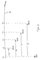
- FIG. 2 is a timing diagram illustrating the operation of the mobile telephone of FIG. 1 ;
- FIG. 3 shows, schematically, a modified version of the telephone of FIG. 1 .
- FIG. 1 shows a mobile telephone 10 which is capable of interacting with basestations, such as 11 and 13 , in a mobile telephone network 12 organised according to the UMTS standard and in a mobile telephone network 14 organised according to the GSM standard.
- the structure of the mobile telephone 10 is not shown in detail in FIG. 1 which schematically illustrates only the processes within the telephone that contribute towards the invention.
- the mobile telephone 10 comprises a GSM subsystem 16 for performing the processing operations that are necessary when communicating with a GSM network, such as network 14 .
- the mobile telephone 10 also comprises a UMTS subsystem 18 for performing the processing operations that are necessary when communicating with a UMTS network, such as network 12 .
- Each of the processing subsystems 16 and 18 is configured to generate signals for transmission from an antenna 20 of the telephone 10 and also to process signals received by the telephone 10 through the antenna 20 .
- the subsystems 16 and 18 share some of the hardware of the telephone 10 , including a clock 24 .
- Clock 24 contains a crystal oscillator for the purpose of generating the clock signal 23 .
- the crystal oscillator is arranged such that the clock signal 23 is at the frequency required by the UMTS subsystem 18 to perform UMTS tasks.
- the UMTS subsystem 18 times and schedules UMTS tasks by using the clock signal 23 directly.
- the clock signal 23 conforms to the UMTS standard so it cannot be used directly in the control of GSM operation of the mobile telephone 10 because the GSM standard demands a clock signal at a different frequency.
- the telephone 10 contains a scheduler 22 that interacts with the clock signal 23 .
- the scheduler 22 uses the clock signal 23 as a reference signal to calculate the moments when certain actions must be begun or stopped by the GSM subsystem 16 . Based on the calculated event timings, the scheduler can send commands to the GSM subsystem 16 to cause GSM tasks to be carried out at the correct times.
- the GSM tasks are not controlled directly by a master clock signal but on the contrary the GSM subsystem 16 receives commands to perform the required GSM tasks at the correct times.
- FIG. 2 illustrates the clock signal 23 extending forward in time from an arbitrary origin t 0 .
- FIG. 2 illustrates a situation where the mobile telephone 10 can acquire signals from four basestations in its vicinity. Two of these basestations form part of a UMTS network and are labelled UMTS#1 and UMTS#2. The other two of these basestations form part of a GSM network and are labelled GSM#1 and GSM#2.
- the mobile telephone 10 is initially operating in the UMTS mode and that it first establishes a link to UMTS#2.
- the UMTS core 18 determines that the boundary of the frame structure of the signals from basestation UMTS#2 occurs at time t 3 . Therefore, the UMTS subsystem 18 records offset C indicating the position of t 3 relative to t 0 so that the UMTS subsystem 18 has a record of the frame structure of the signals of basestation UMTS#2.
- the appropriate UMTS task can be scheduled to commence at the appropriate time by taking offset C into account.
- the UMTS subsystem 18 can acquire signals from basestation UMTS#1 and determine an offset A indicating the position t 1 of the boundary of the frame structure of the signals from the basestation UMTS#1 relative to the arbitrary origin t 0 of clock signal 23 .
- the GSM subsystem 16 can acquire signals from basestations GSM#1 and GSM#2 and process them under commands from the scheduler 22 to determine offsets B and D indicating the boundaries t 2 and t 4 of the frame structures of the signals from GSM#1 and GSM#2 respectively relative to the arbitrary origin t 0 of the clock signal 23 .
- the telephone 10 When linked to basestation UMTS#2, the telephone 10 will monitor the other basestations UMTS#1, GSM#1 and GSM#2 in the vicinity. Primarily, this monitoring is done to determine whether better communications can be achieved (e.g. with fewer errors) by using a communications link to a different basestation.
- FIG. 3 shows a modified version 10 a of the telephone of FIG. 1 .
- the clock signal is abstracted from the telecommunications standards used by the subsystems 16 and 18 and a modified scheduler 22 a uses the clock signal to deduce event timings for controlling both the UMTS subsystem 18 and the GSM subsystem 16 .
- the clock signal 23 must be of sufficiently high frequency so that it can accurately time its issuing of commands to the UMTS and GSM subsystems within the timing error tolerances of those standards.
- the clock 24 produces a signal at 19.2 MHz, which simplifies the calculation of event times by the scheduler 22 a because it is 5 times the UMTS chip rate and 86 times the 200 kHz radio channel spacing used in GSM.
Abstract
Description
Claims (9)
Applications Claiming Priority (3)
| Application Number | Priority Date | Filing Date | Title |
|---|---|---|---|
| GB0404194.3 | 2004-02-25 | ||
| GBGB0404194.3A GB0404194D0 (en) | 2004-02-25 | 2004-02-25 | Wireless communication device and method of operating the same |
| PCT/GB2005/000500 WO2005084050A1 (en) | 2004-02-25 | 2005-02-10 | Wireless multimode communication device using a single clock signal and method of operating the same |
Publications (2)
| Publication Number | Publication Date |
|---|---|
| US20070197204A1 US20070197204A1 (en) | 2007-08-23 |
| US7689246B2 true US7689246B2 (en) | 2010-03-30 |
Family
ID=32050859
Family Applications (1)
| Application Number | Title | Priority Date | Filing Date |
|---|---|---|---|
| US10/590,709 Active 2026-06-29 US7689246B2 (en) | 2004-02-25 | 2005-02-10 | Wireless communication device using a single clock signal and method of operating the same |
Country Status (7)
| Country | Link |
|---|---|
| US (1) | US7689246B2 (en) |
| EP (1) | EP1719370B1 (en) |
| KR (1) | KR101136013B1 (en) |
| CN (1) | CN1939077B (en) |
| GB (1) | GB0404194D0 (en) |
| TW (1) | TWI272027B (en) |
| WO (1) | WO2005084050A1 (en) |
Cited By (2)
| Publication number | Priority date | Publication date | Assignee | Title |
|---|---|---|---|---|
| US20090128213A1 (en) * | 2007-11-19 | 2009-05-21 | Broadcom Corporation | Integrated circuit clock structure |
| US9357414B2 (en) | 2008-12-10 | 2016-05-31 | Samsung Electronics Co., Ltd. | Apparatus and method for inter-rat measurement in a multi mode terminal station |
Families Citing this family (16)
| Publication number | Priority date | Publication date | Assignee | Title |
|---|---|---|---|---|
| US9026070B2 (en) * | 2003-12-18 | 2015-05-05 | Qualcomm Incorporated | Low-power wireless diversity receiver with multiple receive paths |
| US9450665B2 (en) * | 2005-10-19 | 2016-09-20 | Qualcomm Incorporated | Diversity receiver for wireless communication |
| CN101132625A (en) * | 2006-08-20 | 2008-02-27 | 法国电信公司 | Multi-mode radio time scheduling method based on SDR |
| US9178669B2 (en) | 2011-05-17 | 2015-11-03 | Qualcomm Incorporated | Non-adjacent carrier aggregation architecture |
| US9252827B2 (en) | 2011-06-27 | 2016-02-02 | Qualcomm Incorporated | Signal splitting carrier aggregation receiver architecture |
| US9154179B2 (en) | 2011-06-29 | 2015-10-06 | Qualcomm Incorporated | Receiver with bypass mode for improved sensitivity |
| US8774334B2 (en) | 2011-11-09 | 2014-07-08 | Qualcomm Incorporated | Dynamic receiver switching |
| US9172402B2 (en) | 2012-03-02 | 2015-10-27 | Qualcomm Incorporated | Multiple-input and multiple-output carrier aggregation receiver reuse architecture |
| US9362958B2 (en) | 2012-03-02 | 2016-06-07 | Qualcomm Incorporated | Single chip signal splitting carrier aggregation receiver architecture |
| US9118439B2 (en) | 2012-04-06 | 2015-08-25 | Qualcomm Incorporated | Receiver for imbalanced carriers |
| US9154356B2 (en) | 2012-05-25 | 2015-10-06 | Qualcomm Incorporated | Low noise amplifiers for carrier aggregation |
| US9867194B2 (en) | 2012-06-12 | 2018-01-09 | Qualcomm Incorporated | Dynamic UE scheduling with shared antenna and carrier aggregation |
| US9300420B2 (en) | 2012-09-11 | 2016-03-29 | Qualcomm Incorporated | Carrier aggregation receiver architecture |
| US9543903B2 (en) | 2012-10-22 | 2017-01-10 | Qualcomm Incorporated | Amplifiers with noise splitting |
| US8995591B2 (en) | 2013-03-14 | 2015-03-31 | Qualcomm, Incorporated | Reusing a single-chip carrier aggregation receiver to support non-cellular diversity |
| US10177722B2 (en) | 2016-01-12 | 2019-01-08 | Qualcomm Incorporated | Carrier aggregation low-noise amplifier with tunable integrated power splitter |
Citations (19)
| Publication number | Priority date | Publication date | Assignee | Title |
|---|---|---|---|---|
| US6219564B1 (en) * | 1996-12-12 | 2001-04-17 | Nec Corporation | Time base alignment for digital mobile phones |
| WO2001086977A2 (en) | 2000-05-05 | 2001-11-15 | Tantivy Communications, Inc. | Wireless channel allocation in a base station processor |
| EP1162754A2 (en) | 2000-06-06 | 2001-12-12 | Matsushita Electric Industrial Co., Ltd. | Multi-mode cellular phone terminal |
| EP1213830A1 (en) | 2000-12-07 | 2002-06-12 | Motorola, Inc. | Multi-mode radio communications device using a common reference oscillator |
| US6473607B1 (en) * | 1998-06-01 | 2002-10-29 | Broadcom Corporation | Communication device with a self-calibrating sleep timer |
| US20030003951A1 (en) * | 2001-06-28 | 2003-01-02 | Alcatel | Method of switching from a first mobile radio mode to a second mobile radio mode and an associated multimode mobile terminal |
| US20030157912A1 (en) * | 2002-02-21 | 2003-08-21 | Simon Atkinson | 3G radio |
| US20030169825A1 (en) * | 2000-09-14 | 2003-09-11 | Dietmar Wenzel | Signal processor and method for the system-independent digital generation of mobile communication transmit signals of different mobile radio standards |
| US20030214916A1 (en) * | 2002-05-16 | 2003-11-20 | Charbel Khawand | Method and apparatus for arbitrating transmit events in a multimode communication device |
| WO2004004389A1 (en) | 2002-06-26 | 2004-01-08 | Qualcomm, Incorporated | Timer-based sleep for terminals in wireless communication systems |
| US6707822B1 (en) | 2000-01-07 | 2004-03-16 | Agere Systems Inc. | Multi-session asymmetric digital subscriber line buffering and scheduling apparatus and method |
| US6785352B1 (en) * | 1999-02-19 | 2004-08-31 | Nokia Mobile Phones Ltd. | Method and circuit arrangement for implementing inter-system synchronization in a multimode device |
| EP1458111A1 (en) | 2003-03-11 | 2004-09-15 | Sony Ericsson Mobile Communications AB | Multi-band frequency synthesizer |
| US6895255B1 (en) * | 2000-10-20 | 2005-05-17 | Symbol Technologies, Inc. | Dual mode wireless data communications |
| US7046649B2 (en) * | 2000-01-20 | 2006-05-16 | Agere Systems Inc. | Interoperability for bluetooth/IEEE 802.11 |
| US7245725B1 (en) * | 2001-05-17 | 2007-07-17 | Cypress Semiconductor Corp. | Dual processor framer |
| US7260068B2 (en) * | 2003-01-23 | 2007-08-21 | Mediatek Inc. | Method for switching a time frame based mobile unit to a sleep mode |
| US7362188B2 (en) * | 2003-06-04 | 2008-04-22 | Texas Instruments Incorporated | System-on-a-chip (SoC) clock management—a scalable clock distribution approach |
| US7433709B2 (en) * | 2002-04-12 | 2008-10-07 | Nec Corporation | Method of calibrating clocks for two independent radio access technologies without the use of additional hardware |
-
2004
- 2004-02-25 GB GBGB0404194.3A patent/GB0404194D0/en not_active Ceased
-
2005
- 2005-02-10 KR KR1020067017204A patent/KR101136013B1/en not_active IP Right Cessation
- 2005-02-10 WO PCT/GB2005/000500 patent/WO2005084050A1/en not_active Application Discontinuation
- 2005-02-10 CN CN2005800055785A patent/CN1939077B/en not_active Expired - Fee Related
- 2005-02-10 US US10/590,709 patent/US7689246B2/en active Active
- 2005-02-10 EP EP05708323A patent/EP1719370B1/en not_active Not-in-force
- 2005-02-15 TW TW094104265A patent/TWI272027B/en not_active IP Right Cessation
Patent Citations (23)
| Publication number | Priority date | Publication date | Assignee | Title |
|---|---|---|---|---|
| US6219564B1 (en) * | 1996-12-12 | 2001-04-17 | Nec Corporation | Time base alignment for digital mobile phones |
| US6473607B1 (en) * | 1998-06-01 | 2002-10-29 | Broadcom Corporation | Communication device with a self-calibrating sleep timer |
| US6785352B1 (en) * | 1999-02-19 | 2004-08-31 | Nokia Mobile Phones Ltd. | Method and circuit arrangement for implementing inter-system synchronization in a multimode device |
| US6707822B1 (en) | 2000-01-07 | 2004-03-16 | Agere Systems Inc. | Multi-session asymmetric digital subscriber line buffering and scheduling apparatus and method |
| US7046649B2 (en) * | 2000-01-20 | 2006-05-16 | Agere Systems Inc. | Interoperability for bluetooth/IEEE 802.11 |
| WO2001086977A2 (en) | 2000-05-05 | 2001-11-15 | Tantivy Communications, Inc. | Wireless channel allocation in a base station processor |
| EP1162754A2 (en) | 2000-06-06 | 2001-12-12 | Matsushita Electric Industrial Co., Ltd. | Multi-mode cellular phone terminal |
| US7035596B2 (en) * | 2000-06-06 | 2006-04-25 | Matsushita Electric Industrial Co., Ltd. | Multi-mode cellular phone terminal |
| US20030169825A1 (en) * | 2000-09-14 | 2003-09-11 | Dietmar Wenzel | Signal processor and method for the system-independent digital generation of mobile communication transmit signals of different mobile radio standards |
| US6895255B1 (en) * | 2000-10-20 | 2005-05-17 | Symbol Technologies, Inc. | Dual mode wireless data communications |
| EP1213830A1 (en) | 2000-12-07 | 2002-06-12 | Motorola, Inc. | Multi-mode radio communications device using a common reference oscillator |
| US20040037379A1 (en) * | 2000-12-07 | 2004-02-26 | Nadim Khlat | Multi-mode radio communications device using a common reference oscillator |
| US7245725B1 (en) * | 2001-05-17 | 2007-07-17 | Cypress Semiconductor Corp. | Dual processor framer |
| US20030003951A1 (en) * | 2001-06-28 | 2003-01-02 | Alcatel | Method of switching from a first mobile radio mode to a second mobile radio mode and an associated multimode mobile terminal |
| US6959201B2 (en) | 2001-06-28 | 2005-10-25 | Alcatel | Method of switching from a first mobile radio mode to a second mobile radio mode and an associated multimode mobile terminal |
| CN1400835A (en) | 2001-06-28 | 2003-03-05 | 阿尔卡塔尔公司 | Multiple-mode radio communication method and terminal |
| US20030157912A1 (en) * | 2002-02-21 | 2003-08-21 | Simon Atkinson | 3G radio |
| US7433709B2 (en) * | 2002-04-12 | 2008-10-07 | Nec Corporation | Method of calibrating clocks for two independent radio access technologies without the use of additional hardware |
| US20030214916A1 (en) * | 2002-05-16 | 2003-11-20 | Charbel Khawand | Method and apparatus for arbitrating transmit events in a multimode communication device |
| WO2004004389A1 (en) | 2002-06-26 | 2004-01-08 | Qualcomm, Incorporated | Timer-based sleep for terminals in wireless communication systems |
| US7260068B2 (en) * | 2003-01-23 | 2007-08-21 | Mediatek Inc. | Method for switching a time frame based mobile unit to a sleep mode |
| EP1458111A1 (en) | 2003-03-11 | 2004-09-15 | Sony Ericsson Mobile Communications AB | Multi-band frequency synthesizer |
| US7362188B2 (en) * | 2003-06-04 | 2008-04-22 | Texas Instruments Incorporated | System-on-a-chip (SoC) clock management—a scalable clock distribution approach |
Cited By (2)
| Publication number | Priority date | Publication date | Assignee | Title |
|---|---|---|---|---|
| US20090128213A1 (en) * | 2007-11-19 | 2009-05-21 | Broadcom Corporation | Integrated circuit clock structure |
| US9357414B2 (en) | 2008-12-10 | 2016-05-31 | Samsung Electronics Co., Ltd. | Apparatus and method for inter-rat measurement in a multi mode terminal station |
Also Published As
| Publication number | Publication date |
|---|---|
| CN1939077A (en) | 2007-03-28 |
| WO2005084050A1 (en) | 2005-09-09 |
| KR20060135779A (en) | 2006-12-29 |
| EP1719370A1 (en) | 2006-11-08 |
| CN1939077B (en) | 2011-09-07 |
| US20070197204A1 (en) | 2007-08-23 |
| GB0404194D0 (en) | 2004-03-31 |
| KR101136013B1 (en) | 2012-04-24 |
| TWI272027B (en) | 2007-01-21 |
| EP1719370B1 (en) | 2012-08-15 |
| TW200529686A (en) | 2005-09-01 |
Similar Documents
| Publication | Publication Date | Title |
|---|---|---|
| US7689246B2 (en) | Wireless communication device using a single clock signal and method of operating the same | |
| JP4634370B2 (en) | Method and apparatus for handover between radio systems | |
| CN101378355B (en) | Arbitration circuit and method, and wireless device using the same | |
| US9037089B2 (en) | Multi-radio coexistence | |
| TWI477178B (en) | Intelligent resource control in multiple sim user equipment | |
| EP2605557A1 (en) | Virtual modem suspension handler in a multiple SIM user equipement | |
| CN101874386A (en) | Time multiplexing for coexistence within multiple communication systems | |
| CN103430618A (en) | Method and apparatus for interference identification on configuration of LTE and BT | |
| TW201338589A (en) | Periodic registration updates for multiple SIM user equipment | |
| EP2163005B1 (en) | Method and system for synchronization of at least two terminal communication systems and at least one counterpart communication station within a multi-standard wireless communication system | |
| EP2036374B1 (en) | Enhancing interoperatibility among radio protocols of a multimode device | |
| US7907965B2 (en) | Apparatus and method for controlling the power consumption of a combined UMTS/GSM/EDGE radio station | |
| US20060217139A1 (en) | Method and Device for Controlling Combined UMTS/GSM/EDGE Radio Systems | |
| EP0856951B1 (en) | Operating system interface for use with multitasking GSM protocol stacks | |
| US6760586B1 (en) | System and method for processing a handover of digital enhanced cordless telecommunication (DECT) line cards in a switching system | |
| EP2074759B1 (en) | Resource sharing | |
| EP2070216A1 (en) | Control of schedulation | |
| CN111897645B (en) | Multimode chip and terminal device | |
| US7340633B2 (en) | Method for automatically detecting the clock frequency of a system clock pulse for the configuration of a peripheral device | |
| US6157629A (en) | CDMA mobile communication system of automatically changing frequency and method thereof | |
| US7555669B2 (en) | Timing vector program mechanism | |
| CN110831071B (en) | Information processing method and network equipment | |
| JP2815807B2 (en) | Control channel standby method | |
| CN114915387A (en) | Data transmission method, terminal device, and computer-readable storage medium | |
| WO2011098132A1 (en) | Communication entity with timing generator coupled via a digital protocol to sample-driven further communication entity |
Legal Events
| Date | Code | Title | Description |
|---|---|---|---|
| AS | Assignment |
Owner name: TTPCOM LIMITED,UNITED KINGDOM Free format text: ASSIGNMENT OF ASSIGNORS INTEREST;ASSIGNORS:HERCZOG, EUGENE PASCAL;PATON, NIGEL GOW;SIGNING DATES FROM 20060823 TO 20060824;REEL/FRAME:018252/0937 Owner name: TTPCOM LIMITED, UNITED KINGDOM Free format text: ASSIGNMENT OF ASSIGNORS INTEREST;ASSIGNORS:HERCZOG, EUGENE PASCAL;PATON, NIGEL GOW;REEL/FRAME:018252/0937;SIGNING DATES FROM 20060823 TO 20060824 |
|
| AS | Assignment |
Owner name: MSTAR SEMICONDUCTOR, INC.,CAYMAN ISLANDS Free format text: ASSIGNMENT OF ASSIGNORS INTEREST;ASSIGNOR:TTPCOM, LTD.;REEL/FRAME:022034/0532 Effective date: 20080411 Owner name: MSTAR SEMICONDUCTOR, INC., CAYMAN ISLANDS Free format text: ASSIGNMENT OF ASSIGNORS INTEREST;ASSIGNOR:TTPCOM, LTD.;REEL/FRAME:022034/0532 Effective date: 20080411 |
|
| AS | Assignment |
Owner name: MSTAR SEMICONDUCTOR, INC.,CHINA Free format text: ASSIGNMENT OF ASSIGNORS INTEREST;ASSIGNOR:MSTAR SEMICONDUCTOR, INC.;REEL/FRAME:022043/0104 Effective date: 20081216 Owner name: MSTAR FRANCE SAS,FRANCE Free format text: ASSIGNMENT OF ASSIGNORS INTEREST;ASSIGNOR:MSTAR SEMICONDUCTOR, INC.;REEL/FRAME:022043/0104 Effective date: 20081216 Owner name: MSTAR SOFTWARE R&D (SHENZHEN) LTD.,CHINA Free format text: ASSIGNMENT OF ASSIGNORS INTEREST;ASSIGNOR:MSTAR SEMICONDUCTOR, INC.;REEL/FRAME:022043/0104 Effective date: 20081216 Owner name: MSTAR SEMICONDUCTOR, INC.,CAYMAN ISLANDS Free format text: ASSIGNMENT OF ASSIGNORS INTEREST;ASSIGNOR:MSTAR SEMICONDUCTOR, INC.;REEL/FRAME:022043/0104 Effective date: 20081216 Owner name: MSTAR SEMICONDUCTOR, INC., CHINA Free format text: ASSIGNMENT OF ASSIGNORS INTEREST;ASSIGNOR:MSTAR SEMICONDUCTOR, INC.;REEL/FRAME:022043/0104 Effective date: 20081216 Owner name: MSTAR FRANCE SAS, FRANCE Free format text: ASSIGNMENT OF ASSIGNORS INTEREST;ASSIGNOR:MSTAR SEMICONDUCTOR, INC.;REEL/FRAME:022043/0104 Effective date: 20081216 Owner name: MSTAR SOFTWARE R&D (SHENZHEN) LTD., CHINA Free format text: ASSIGNMENT OF ASSIGNORS INTEREST;ASSIGNOR:MSTAR SEMICONDUCTOR, INC.;REEL/FRAME:022043/0104 Effective date: 20081216 Owner name: MSTAR SEMICONDUCTOR, INC., CAYMAN ISLANDS Free format text: ASSIGNMENT OF ASSIGNORS INTEREST;ASSIGNOR:MSTAR SEMICONDUCTOR, INC.;REEL/FRAME:022043/0104 Effective date: 20081216 |
|
| STCF | Information on status: patent grant |
Free format text: PATENTED CASE |
|
| CC | Certificate of correction | ||
| FPAY | Fee payment |
Year of fee payment: 4 |
|
| MAFP | Maintenance fee payment |
Free format text: PAYMENT OF MAINTENANCE FEE, 8TH YEAR, LARGE ENTITY (ORIGINAL EVENT CODE: M1552) Year of fee payment: 8 |
|
| AS | Assignment |
Owner name: MEDIATEK INC., TAIWAN Free format text: MERGER;ASSIGNOR:MSTAR SEMICONDUCTOR, INC.;REEL/FRAME:054595/0404 Effective date: 20190114 Owner name: MEDIATEK INC., TAIWAN Free format text: MERGER;ASSIGNOR:MSTAR SEMICONDUCTOR, INC. (CAYMAN ISLANDS);REEL/FRAME:054595/0227 Effective date: 20140214 Owner name: MEDIATEK INC., TAIWAN Free format text: ASSIGNMENT OF ASSIGNORS INTEREST;ASSIGNOR:MSTAR FRANCE SAS;REEL/FRAME:054592/0876 Effective date: 20200630 |
|
| AS | Assignment |
Owner name: MEDIATEK INC., TAIWAN Free format text: ASSIGNMENT OF ASSIGNORS INTEREST;ASSIGNOR:MSTAR SOFTWARE R&D (SHENZHEN) LTD.;REEL/FRAME:054711/0715 Effective date: 20191231 |
|
| AS | Assignment |
Owner name: XUESHAN TECHNOLOGIES INC., CANADA Free format text: ASSIGNMENT OF ASSIGNORS INTEREST;ASSIGNOR:MEDIATEK INC.;REEL/FRAME:055443/0818 Effective date: 20201223 |
|
| MAFP | Maintenance fee payment |
Free format text: PAYMENT OF MAINTENANCE FEE, 12TH YEAR, LARGE ENTITY (ORIGINAL EVENT CODE: M1553); ENTITY STATUS OF PATENT OWNER: LARGE ENTITY Year of fee payment: 12 |