US9277425B2 - Systems and methods for automatic frequency control for mobile communication systems - Google Patents
Systems and methods for automatic frequency control for mobile communication systems Download PDFInfo
- Publication number
- US9277425B2 US9277425B2 US13/783,568 US201313783568A US9277425B2 US 9277425 B2 US9277425 B2 US 9277425B2 US 201313783568 A US201313783568 A US 201313783568A US 9277425 B2 US9277425 B2 US 9277425B2
- Authority
- US
- United States
- Prior art keywords
- signal
- communication device
- frequency
- reference clock
- clock signal
- Prior art date
- Legal status (The legal status is an assumption and is not a legal conclusion. Google has not performed a legal analysis and makes no representation as to the accuracy of the status listed.)
- Active, expires
Links
- 238000000034 method Methods 0.000 title claims abstract description 20
- 238000010295 mobile communication Methods 0.000 title claims abstract description 11
- 238000004891 communication Methods 0.000 claims abstract description 112
- 230000001413 cellular effect Effects 0.000 claims description 8
- 238000010586 diagram Methods 0.000 description 6
- 230000005540 biological transmission Effects 0.000 description 4
- 239000013078 crystal Substances 0.000 description 3
- 230000010355 oscillation Effects 0.000 description 3
- 238000005516 engineering process Methods 0.000 description 2
- 230000007246 mechanism Effects 0.000 description 2
- IRLPACMLTUPBCL-KQYNXXCUSA-N 5'-adenylyl sulfate Chemical compound C1=NC=2C(N)=NC=NC=2N1[C@@H]1O[C@H](COP(O)(=O)OS(O)(=O)=O)[C@@H](O)[C@H]1O IRLPACMLTUPBCL-KQYNXXCUSA-N 0.000 description 1
- 230000001934 delay Effects 0.000 description 1
- 230000000694 effects Effects 0.000 description 1
- 230000004044 response Effects 0.000 description 1
Images


Classifications
-
- H—ELECTRICITY
- H04—ELECTRIC COMMUNICATION TECHNIQUE
- H04W—WIRELESS COMMUNICATION NETWORKS
- H04W24/00—Supervisory, monitoring or testing arrangements
- H04W24/02—Arrangements for optimising operational condition
-
- H—ELECTRICITY
- H03—ELECTRONIC CIRCUITRY
- H03J—TUNING RESONANT CIRCUITS; SELECTING RESONANT CIRCUITS
- H03J7/00—Automatic frequency control; Automatic scanning over a band of frequencies
- H03J7/02—Automatic frequency control
- H03J7/04—Automatic frequency control where the frequency control is accomplished by varying the electrical characteristics of a non-mechanically adjustable element or where the nature of the frequency controlling element is not significant
-
- H—ELECTRICITY
- H04—ELECTRIC COMMUNICATION TECHNIQUE
- H04W—WIRELESS COMMUNICATION NETWORKS
- H04W88/00—Devices specially adapted for wireless communication networks, e.g. terminals, base stations or access point devices
- H04W88/02—Terminal devices
- H04W88/06—Terminal devices adapted for operation in multiple networks or having at least two operational modes, e.g. multi-mode terminals
Definitions
- the technology described in this patent document relates generally to wireless communication and more particularly to mobile communication systems.
- Wireless communication systems such as cellular phones, can be used in many wireless networks implementing different technologies, e.g., Code Division Multiple Access (CDMA), Global System for Mobile Communications (GSM), General Packet Radio Service (GPRS), Evolution-Data Optimized (EV-DO), Enhanced Data Rates for GSM Evolution (EDGE), 3GSM, Digital Enhanced Cordless Telecommunications (DECT), Digital AMPS (IS-136/TDMA), and Integrated Digital Enhanced Network (iDEN), etc.
- CDMA Code Division Multiple Access
- GSM Global System for Mobile Communications
- GPRS General Packet Radio Service
- EV-DO Evolution-Data Optimized
- EDGE Enhanced Data Rates for GSM Evolution
- 3GSM Third Generation
- DECT Digital Enhanced Cordless Telecommunications
- iDEN Integrated Digital Enhanced Network
- a wireless communication system e.g., a cellular phone
- a base station of a wireless network there is usually certain deviation between the receiving frequency of the wireless communication system and the transmitting frequency of the base station.
- Such frequency deviation usually comprises local oscillation frequency deviation and Doppler frequency shift.
- the local oscillation frequency deviation generally includes the difference between a local oscillation frequency of the wireless communication system and the transmitting frequency of the base station.
- Doppler frequency shift is often caused by the movement of the wireless communication system, and thus is associated with the speed and the direction at which the wireless communication system is moving relative to the base station.
- An example mobile communication system includes a first communication device configured to communicate with a first wireless network and generate a reference signal for determining a first frequency deviation between the first communication device and the first wireless network, and a second communication device configured to communicate with a second wireless network and determine a second frequency deviation between the second communication device and the second wireless network based at least in part on the reference signal.
- a method for communicating with multiple wireless networks using a mobile communication system.
- a first communication device in the mobile communication system communicates with a first wireless network.
- a reference signal is generated.
- a first frequency deviation between the first communication device and the first wireless network is determined.
- a second communication device in the mobile communication system communicates with a second wireless network.
- a second frequency deviation between the second communication device and the second wireless network is determined based at least in part on the reference signal.
- FIG. 1 illustrates an example wireless communication system communicating with multiple wireless networks.
- FIG. 2 illustrates an example wireless communication system communicating with two wireless networks.
- FIG. 3 illustrates an example of some components in the wireless communication system as shown in FIG. 2 .
- FIG. 4 illustrates an example of certain components in the wireless communication system as shown in FIG. 3 .
- FIG. 5 shows a timing diagram illustrating an example operation of the wireless communication system as shown in FIGS. 2-4 .
- FIG. 6 shows a timing diagram illustrating another example operation of the wireless communication system as shown in FIGS. 2-4 .
- FIGS. 7-9 show timing diagrams illustrating example operations of the wireless communication system as shown in FIGS. 2-4 for timing control of adjusting the reference clock signal.
- a wireless communication system e.g., a cellular phone
- normal communication between the wireless communication system and the wireless network may be maintained when the frequency deviation between the receiving frequency of the wireless communication system and the transmitting frequency of a base station of the wireless network is controlled within a certain range.
- a wireless communication system often tracks and controls such frequency deviation between the wireless communication system and the wireless network.
- the wireless communication system may include a crystal oscillator that generates a reference clock signal indicative of the receiving frequency of the wireless communication system.
- the frequency deviation between the wireless communication system and the wireless network may be determined by comparing the frequency of the reference clock signal with the transmitting frequency of a base station of the wireless network.
- the reference clock signal may then be adjusted in order to reduce the frequency deviation.
- a wireless communication system may include multiple communication devices (e.g., chips) to communicate with multiple wireless networks respectively.
- the frequency deviations with respect to these wireless networks are often very different. For example, when the wireless communication system moves, the speeds and the directions at which the wireless communication system moves vary relative to the base stations of these wireless networks, and thus the Doppler shifts are different. Therefore, it can be hard to control the frequency deviations with respect to these wireless networks simultaneously by adjusting a single reference clock signal in response to each of these different frequency deviations.
- each communication device in the wireless communication system may have its own crystal oscillator and associated circuit components, so that multiple reference clock signals may be generated for the wireless networks respectively, but the system costs will increase.
- FIG. 1 illustrates an example wireless communication system communicating with multiple wireless networks.
- the wireless communication system 100 e.g., a single cellular phone
- the device 102 generates the reference clock signal 106 indicative of a receiving frequency of the device 102 , and adjusts the reference clock signal 106 to keep a frequency deviation between the device 102 and a wireless network with which the device 102 communicates within a predetermined range.
- one of the devices 104 1 , . . . , and 104 n determines a frequency deviation with respect to another wireless network with which the device communicates based at least in part on the reference clock signal 106 . Then, the device (e.g., 104 1 , . . . , or 104 n ) operates to keep the frequency deviation within a predetermined range without changing the reference clock signal 106 . For example, the device (e.g., 104 1 , . . . , or 104 n ) may adjust the receiving (or transmitting) frequency through internal mechanisms.
- FIG. 2 illustrates an example wireless communication system 200 (e.g., a single cellular phone) that includes two communication devices 202 and 204 for communicating (e.g., receiving/transmitting signals) with two wireless networks ⁇ and ⁇ respectively through one or more antennas 250 .
- the communication devices 202 and 204 depicted in FIG. 2 may, for example, be the device 102 and one of the devices 104 1 , . . . , and 104 n respectively.
- the device 202 generates a reference clock signal 224 using a reference-signal generator 226 (e.g., a crystal oscillator), and adjusts the reference clock signal 224 to keep a frequency deviation between the device 202 and the wireless network ⁇ with which the device 202 communicates within a predetermined range.
- the device 204 receives the reference clock signal 224 and determines a frequency deviation between the device 204 and the wireless network ⁇ based at least in part on the reference clock signal 224 . Then, the device 204 operates to keep the frequency deviation within a predetermined range.
- the device 202 uses an initial receiving frequency. If the deviation between the initial receiving frequency and the transmitting frequency of a base station of the wireless network ⁇ is within a certain range (e.g., 1 parts per million), the device 202 can achieve synchronization and access to the wireless network ⁇ . As long as the frequency deviation is kept within the range, the device 202 can continue to receive signals from the base station.
- a certain range e.g. 1 parts per million
- a power amplifier 208 in the device 202 receives a signal 228 from the wireless network ⁇ through the antennas 250 and outputs an amplified signal 232 to a multiplexer 220 .
- the reference-signal generator 226 outputs the reference clock signal 224 (e.g., 26 MHz) to a phase-locked loop 210 which outputs a signal 234 indicative of the initial receiving frequency (e.g., about 2.6 GHz) to the multiplexer 220 .
- the phase of the signal 234 is related to the reference clock signal 224 .
- a frequency deviation between the device 202 and the wireless network ⁇ may be determined based on the amplified signal 232 and the signal 234 .
- a signal-processing component 216 (e.g., a digital-to-analog converter) outputs a signal 244 to the reference-signal generator 226 to adjust the reference clock signal 224 in order to keep the frequency deviation between the device 202 and the wireless network ⁇ within the predetermined range.
- the phase-locked loop 210 outputs the reference clock signal 224 to a phase-locked loop 212 in the device 204 which outputs a signal 236 indicative of a receiving frequency of the device 204 to a multiplexer 222 .
- a power amplifier 214 in the device 204 receives a signal 238 from the wireless network ⁇ through the antennas 250 and outputs an amplified signal 240 to the multiplexer 222 .
- a frequency deviation between the device 204 and the wireless network ⁇ is determined based on the amplified signal 240 and the signal 236 .
- a signal-processing component 218 (e.g., a register) stores the determined frequency deviation and generates a signal 242 to affect the output of the phase-locked loop 212 so as to keep the frequency deviation between the device 204 and the wireless network ⁇ within the predetermined range.
- the antennas 250 may include two antennas for the devices 202 and 204 respectively.
- the communication devices 202 and 204 may each include a radio-frequency (RF) communication component for communicating with a wireless network and a baseband component for determining a frequency deviation.
- RF radio-frequency
- the device 202 includes a RF communication component 260 and a baseband component 262
- the device 204 includes a RF communication component 264 and a baseband component 266 .
- the baseband component 262 outputs a signal 268 indicative of a frequency deviation (e.g., AFC A, n ) between the device 202 and the wireless network ⁇ to the signal-processing component 216 (e.g., a digital-to-analog converter) which may affect the reference-signal generator 226 to control the frequency deviation (e.g., AFC A, n ) for the device 202 .
- a frequency deviation e.g., AFC A, n
- the signal-processing component 216 e.g., a digital-to-analog converter
- the baseband component 266 outputs a signal 270 indicative of a frequency deviation (e.g., AFC B, m ) between the device 204 and the wireless network ⁇ to the signal-processing component 218 (e.g., a register) which may affect the phase-locked loop 212 to control the frequency deviation (e.g., AFC B, m ) for the device 204 .
- a frequency deviation e.g., AFC B, m
- the signal-processing component 218 e.g., a register
- FIG. 4 illustrates an example of certain components in the wireless communication system 200 .
- the RF communication component 260 further includes an analog-to-digital/digital-to-analog (AD/DA) converter 280
- the baseband component 262 includes a modulator/encoder 282 , a demodulator/decoder 284 and a frequency-deviation estimator 286 .
- the AD/DA converter 280 may output a processed signal 252 to the demodulator/decoder 284 which generates a demodulated signal 254 for the frequency-deviation estimator 286 to determine a frequency deviation for the device 202 .
- the frequency-deviation estimator 286 may use a look-up table to generate a voltage value based on a residual frequency-deviation value.
- the signal-processing component 216 may receive the signal 268 representative of the generated voltage value for controlling the reference-signal generator 226 to keep the frequency deviation within the predetermined range.
- the AD/DA converter 280 may process modulated/encoded signals generated from the modulator/encoder 282 for transmission by the device 202 .
- the RF communication component 264 further includes an AD/DA converter 288 .
- the baseband component 266 includes a modulator/encoder 290 , a demodulator/decoder 292 and a frequency-deviation estimator 294 to perform similar operations as the baseband component 262 .
- the baseband components 262 and 266 may be built on a same baseband chip.
- the RF communication components 260 and 264 may share a same frequency-deviation estimator, a same AD/DA converter, a same encoder/modulator, and/or a same demodulator/decoder.
- FIG. 5 shows a timing diagram illustrating an example operation of the wireless communication system 200 .
- the device 202 adjusts the reference clock signal 224 after receiving a signal from the wireless network ⁇ .
- the device 204 determines a frequency deviation with respect to the wireless network ⁇ based at least in part on the reference clock signal 224 .
- the device 202 determines a frequency deviation AFC A, 1 , and adjusts the reference clock signal 224 so as to control the frequency deviation as described above with respect to FIGS. 2-4 .
- the device 204 determines a frequency deviation AFC B, 1 with respect to the wireless network ⁇ based at least in part on the reference clock signal 224 .
- the phase-locked loop 212 may be adjusted based on the determined frequency deviation AFC B, 1 .
- the device 204 After a first reception from the wireless network ⁇ (e.g., R x, B at t 2 ), the device 204 determines another frequency deviation AFC B, 2 based on the received signal and the reference clock signal 224 and stores the determined frequency deviation AFC B, 2 in the signal-processing component 218 (e.g., a register).
- the signal-processing component 218 e.g., a register
- the device 204 In preparation for a second reception (e.g., R x, B at t 3 ), the device 204 needs to determine a frequency deviation (e.g., AFC B, 3 ) with respect to the wireless network ⁇ . As shown in FIG. 5 , the device 202 does not receive signals from the wireless network ⁇ between the times t 2 and t 3 , and thus the reference clock signal 224 is not changed during that time period. Therefore, the frequency deviation AFC B, 3 is the same as the frequency deviation AFC B, 2 . After the second reception, the device 204 determines another frequency deviation AFC B, 4 based on the received signal and the reference clock signal 224 and stores the determined frequency deviation AFC B, 4 in the signal-processing component 218 (e.g., a register).
- the signal-processing component 218 e.g., a register
- FIG. 6 shows a timing diagram illustrating another example operation of the wireless communication system 200 .
- the device 202 adjusts the reference clock signal 224 after each reception from the wireless network ⁇ .
- the device 204 determines a frequency deviation for communication with the wireless network ⁇ , it takes into account preceding changes to the reference clock signal 224 made by the device 202 .
- the device 202 determines a frequency deviation AFC A, 1 , and adjusts the reference clock signal 224 .
- the device 204 determines a frequency deviation AFC B, 1 with respect to the wireless network ⁇ based at least in part on the reference clock signal 224 .
- the phase-locked loop 212 may be adjusted based on the determined frequency deviation AFC B, 1 .
- the device 204 After a first reception from the wireless network ⁇ (e.g., R x, B at t 6 ), the device 204 determines another frequency deviation AFC B, 2 based on the received signal and the reference clock signal 224 and stores the determined frequency deviation AFC B, 2 in the signal-processing component 218 (e.g., a register).
- the signal-processing component 218 e.g., a register
- the device 202 has multiple receptions from the wireless network ⁇ (e.g., R x, A at t 7 , R x, A at t 8 , . . . , R x, A at t 9 ), and further adjusts the reference clock signal 224 after each reception based on determined frequency deviations (e.g., AFC A, 2 , AFC A, 3 , . . . , AFC A, n ).
- the device 204 needs to determine a frequency deviation with respect to the wireless network ⁇ .
- the frequency deviation AFC B, 2 stored in the signal-processing component 218 was determined based on the reference clock signal 224 right after the first reception of the device 202 , without taking into account the changes made by the device 202 subsequently.
- the device 202 determines a frequency deviation AFC A, n+1 , and adjusts the reference clock signal 224 accordingly.
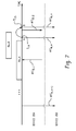
- FIGS. 7-9 show timing diagrams illustrating example operations of the wireless communication system 200 for timing control of adjusting the reference clock signal 224 .
- the device 202 changes the reference clock signal 224 after a reception, it may take a period of time for the reference clock signal 224 to stabilize. If the device 204 communicates with the wireless network ⁇ before the reference clock signal 224 stabilizes, negative effects may be caused to the communication of the device 204 .
- the wireless communication system 200 as shown in FIGS. 2-4 may further include one or more timing engines (e.g., in the baseband component 262 and/or the baseband component 266 ) to monitor the communication status of the device 202 and the device 204 , so as to control the timing of changing the reference clock signal 224 .
- the device 204 begins to receive signals from the wireless network ⁇ (e.g., R x, B ) during a continuous reception of the device 202 from the wireless network ⁇ (e.g., R x, A ), and the reception of the device 204 lasts longer than the reception of the device 202 .
- the device 202 may delay the determination of frequency deviation and the adjustment of the reference clock signal 224 from time t 14 to time t 15 , i.e., after the reception of the device 204 .
- the device 202 delays the determination of frequency deviation and the adjustment of the reference clock signal 224 after a transmission of the device 204 (e.g., T x, B ).
- a continuous reception of the device 204 overlaps two consecutive receptions of the device 202 (i.e., “first reception” and “second reception”). There is neither a determination of frequency deviation nor adjustment of the reference clock signal 224 after the first reception of the device 202 .
- the device 202 determines a frequency reception and adjusts the reference clock signal 224 (e.g., at time t 16 ).
- the systems and methods described herein may be implemented on many different types of processing systems by program code comprising program instructions that are executable by the system processing subsystem. Other implementations may also be used, however, such as firmware or appropriately designed hardware configured to carry out the methods and systems described herein.
- the systems and methods described herein may be implemented in an independent processing engine, as a co-processor, or as a hardware accelerator.
- the systems and methods described herein may be provided on many different types of computer-readable media including computer storage mechanisms (e.g., CD-ROM, diskette, RAM, flash memory, computer's hard drive, etc.) that contain instructions (e.g., software) for use in execution by a processor to perform the methods' operations and implement the systems described herein.
Abstract
Description
AFC B, 3 =AFC B, 2−(AFC A, n −AFC A, 1) (1)
Then, the
AFC B, 4 =AFC B, 3−(AFC A, n+1 −AFC A, n) (2)
Claims (19)
Priority Applications (1)
| Application Number | Priority Date | Filing Date | Title |
|---|---|---|---|
| US13/783,568 US9277425B2 (en) | 2012-03-30 | 2013-03-04 | Systems and methods for automatic frequency control for mobile communication systems |
Applications Claiming Priority (2)
| Application Number | Priority Date | Filing Date | Title |
|---|---|---|---|
| US201261618196P | 2012-03-30 | 2012-03-30 | |
| US13/783,568 US9277425B2 (en) | 2012-03-30 | 2013-03-04 | Systems and methods for automatic frequency control for mobile communication systems |
Publications (2)
| Publication Number | Publication Date |
|---|---|
| US20130260742A1 US20130260742A1 (en) | 2013-10-03 |
| US9277425B2 true US9277425B2 (en) | 2016-03-01 |
Family
ID=49235681
Family Applications (1)
| Application Number | Title | Priority Date | Filing Date |
|---|---|---|---|
| US13/783,568 Active 2034-05-07 US9277425B2 (en) | 2012-03-30 | 2013-03-04 | Systems and methods for automatic frequency control for mobile communication systems |
Country Status (2)
| Country | Link |
|---|---|
| US (1) | US9277425B2 (en) |
| CN (1) | CN103369726B (en) |
Cited By (1)
| Publication number | Priority date | Publication date | Assignee | Title |
|---|---|---|---|---|
| US10509104B1 (en) | 2018-08-13 | 2019-12-17 | Analog Devices Global Unlimited Company | Apparatus and methods for synchronization of radar chips |
Families Citing this family (8)
| Publication number | Priority date | Publication date | Assignee | Title |
|---|---|---|---|---|
| WO2015095986A1 (en) * | 2013-12-24 | 2015-07-02 | Intel IP Corporation | System and method for frequency control loop in mobile device with plurality of sims |
| CN104853382B (en) | 2014-02-18 | 2020-08-25 | 中兴通讯股份有限公司 | Information interaction method, system and base station |
| US20150271836A1 (en) * | 2014-03-21 | 2015-09-24 | Qualcomm Incorporated | Techniques for bearer prioritization and data mapping in multiple connectivity wireless communications |
| CN105101253B (en) * | 2014-05-09 | 2020-04-24 | 上海诺基亚贝尔股份有限公司 | Method, main base station and user equipment used in dual-connection system |
| GB2542739B8 (en) | 2014-08-25 | 2021-05-12 | Quanten Tech Limited | Wireless power transfer system and method |
| JP6169057B2 (en) * | 2014-08-27 | 2017-07-26 | 株式会社Nttドコモ | User device and offset report method |
| CN113014724B (en) * | 2019-12-18 | 2023-04-11 | 深圳市万普拉斯科技有限公司 | Dual-connection mode starting method and device, mobile terminal and readable storage medium |
| CN113613235B (en) * | 2021-07-27 | 2022-12-27 | 展讯通信(上海)有限公司 | Frequency offset adjusting method and device, terminal and network equipment |
Citations (7)
| Publication number | Priority date | Publication date | Assignee | Title |
|---|---|---|---|---|
| US5982831A (en) * | 1996-02-21 | 1999-11-09 | Hewlett-Packard Company | Feed forward method and apparatus for generating a clock signal |
| US6324228B1 (en) * | 1998-12-30 | 2001-11-27 | International Business Machines Corporation | Method and apparatus for robust frequency tracking in strong channel interference using carrier signal relative strength and frequency error |
| US20090042591A1 (en) * | 2007-08-10 | 2009-02-12 | Samsung Electronics Co. Ltd. | Apparatus and method for acquiring synchronization to support multi-frequency in mobile communication terminal |
| US20090088085A1 (en) * | 2007-10-01 | 2009-04-02 | Magnus Nilsson | Apparatus and Methods for Frequency Control in a Multi-Output Frequency Synthesizer |
| US20090225743A1 (en) * | 2008-03-07 | 2009-09-10 | Charles Nicholls | Using a network frequency reference to augment timing synchronization in a wireless base station |
| US20090258628A1 (en) * | 2008-04-14 | 2009-10-15 | Bengt Lindoff | Time-Error and Frequency-Error Correction in a Multi-Carrier Wireless Communications System |
| US20100330931A1 (en) * | 2009-06-24 | 2010-12-30 | Gregory Uehara | System and transceiver clocking to minimize required number of reference sources in multi-function cellular applications including gps |
Family Cites Families (3)
| Publication number | Priority date | Publication date | Assignee | Title |
|---|---|---|---|---|
| US7308063B2 (en) * | 2002-12-20 | 2007-12-11 | Nokia Corporation | Apparatus, and associated method, for effectuating post-FFT correction of fine frequency offset |
| CN100499384C (en) * | 2005-08-05 | 2009-06-10 | 上海明波通信技术有限公司 | Device and method for realizing frequency switch and automatic control of multiple-module mobile communication terminal |
| US20090213946A1 (en) * | 2008-02-25 | 2009-08-27 | Xilinx, Inc. | Partial reconfiguration for a mimo-ofdm communication system |
-
2013
- 2013-03-04 US US13/783,568 patent/US9277425B2/en active Active
- 2013-03-29 CN CN201310117697.6A patent/CN103369726B/en active Active
Patent Citations (7)
| Publication number | Priority date | Publication date | Assignee | Title |
|---|---|---|---|---|
| US5982831A (en) * | 1996-02-21 | 1999-11-09 | Hewlett-Packard Company | Feed forward method and apparatus for generating a clock signal |
| US6324228B1 (en) * | 1998-12-30 | 2001-11-27 | International Business Machines Corporation | Method and apparatus for robust frequency tracking in strong channel interference using carrier signal relative strength and frequency error |
| US20090042591A1 (en) * | 2007-08-10 | 2009-02-12 | Samsung Electronics Co. Ltd. | Apparatus and method for acquiring synchronization to support multi-frequency in mobile communication terminal |
| US20090088085A1 (en) * | 2007-10-01 | 2009-04-02 | Magnus Nilsson | Apparatus and Methods for Frequency Control in a Multi-Output Frequency Synthesizer |
| US20090225743A1 (en) * | 2008-03-07 | 2009-09-10 | Charles Nicholls | Using a network frequency reference to augment timing synchronization in a wireless base station |
| US20090258628A1 (en) * | 2008-04-14 | 2009-10-15 | Bengt Lindoff | Time-Error and Frequency-Error Correction in a Multi-Carrier Wireless Communications System |
| US20100330931A1 (en) * | 2009-06-24 | 2010-12-30 | Gregory Uehara | System and transceiver clocking to minimize required number of reference sources in multi-function cellular applications including gps |
Cited By (1)
| Publication number | Priority date | Publication date | Assignee | Title |
|---|---|---|---|---|
| US10509104B1 (en) | 2018-08-13 | 2019-12-17 | Analog Devices Global Unlimited Company | Apparatus and methods for synchronization of radar chips |
Also Published As
| Publication number | Publication date |
|---|---|
| CN103369726B (en) | 2017-12-01 |
| US20130260742A1 (en) | 2013-10-03 |
| CN103369726A (en) | 2013-10-23 |
Similar Documents
| Publication | Publication Date | Title |
|---|---|---|
| US9277425B2 (en) | Systems and methods for automatic frequency control for mobile communication systems | |
| CN106465317B (en) | Timing advance techniques for large cells | |
| JP5043115B2 (en) | Method and apparatus for efficiently applying frequency correction | |
| JP6392899B2 (en) | Adaptive control of RF low power mode in multi-rate wireless system using device mode | |
| KR101448056B1 (en) | Enhanced multiple sim time tracking | |
| US20150103817A1 (en) | Global time synchronization server for wireless devices | |
| TWI486073B (en) | Wireless communication device capable of efficient radio access technology measurements | |
| KR101004595B1 (en) | System and method of frequency acquisition | |
| RU2607638C1 (en) | Method and device for signal demodulation | |
| CN112911701B (en) | Frequency offset control method and device, terminal and storage medium | |
| EP2036374B1 (en) | Enhancing interoperatibility among radio protocols of a multimode device | |
| WO2015175291A1 (en) | Timing advance techniques for large cells | |
| CN110710310B (en) | Super system frame number determining method, communication method and device | |
| WO2023185808A1 (en) | Cell synchronization method and apparatus | |
| CN111757455A (en) | Method and communication device for adjusting downlink transmission timing | |
| JPH10200471A (en) | Correcting method for doppler effect for radio communication network with mobile object | |
| WO2021134705A1 (en) | Method for determining time synchronization and related product | |
| CN114390662A (en) | Time delay compensation method, device and equipment for TSN reference time | |
| JP2002262356A (en) | Wireless communication terminal | |
| CN114246001A (en) | Wireless communication method, device and communication equipment | |
| US20240121681A1 (en) | Wireless telecommunications network | |
| CN112586056B (en) | Method for self-interference cancellation, terminal device and network device | |
| US20240064672A1 (en) | Method, user equipment, and base station | |
| KR100581080B1 (en) | Apparatus and method for closed-loop frequency synchronization by estimation and compensation of doppler shift in a mobile terminal | |
| CN115225135A (en) | Signal transmission method and device and readable storage medium |
Legal Events
| Date | Code | Title | Description |
|---|---|---|---|
| AS | Assignment |
Owner name: MARVELL WORLD TRADE LTD., BARBADOS Free format text: ASSIGNMENT OF ASSIGNORS INTEREST;ASSIGNOR:MARVELL INTERNATIONAL LTD.;REEL/FRAME:030122/0079 Effective date: 20130227 Owner name: MARVELL INTERNATIONAL LTD., BERMUDA Free format text: ASSIGNMENT OF ASSIGNORS INTEREST;ASSIGNOR:MARVELL TECHNOLOGY (SHANGHAI) LTD.;REEL/FRAME:030122/0024 Effective date: 20130226 Owner name: MARVELL TECHNOLOGY (SHANGHAI) LTD., CHINA Free format text: ASSIGNMENT OF ASSIGNORS INTEREST;ASSIGNORS:YIN, XIAOJUN;YU, SHIYI;REEL/FRAME:030121/0954 Effective date: 20130226 Owner name: MARVELL INTERNATIONAL LTD., BERMUDA Free format text: LICENSE;ASSIGNOR:MARVELL WORLD TRADE LTD.;REEL/FRAME:030122/0126 Effective date: 20130401 |
|
| STCF | Information on status: patent grant |
Free format text: PATENTED CASE |
|
| AS | Assignment |
Owner name: MARVELL INTERNATIONAL LTD., BERMUDA Free format text: ASSIGNMENT OF ASSIGNORS INTEREST;ASSIGNOR:MARVELL WORLD TRADE LTD.;REEL/FRAME:042066/0557 Effective date: 20170418 |
|
| AS | Assignment |
Owner name: ASR MICROELECTRONICS (SHANGHAI) CO. LTD., CHINA Free format text: ASSIGNMENT OF ASSIGNORS INTEREST;ASSIGNOR:MARVELL INTERNATIONAL LTD.;REEL/FRAME:043887/0860 Effective date: 20170828 |
|
| FEPP | Fee payment procedure |
Free format text: ENTITY STATUS SET TO SMALL (ORIGINAL EVENT CODE: SMAL); ENTITY STATUS OF PATENT OWNER: SMALL ENTITY |
|
| MAFP | Maintenance fee payment |
Free format text: PAYMENT OF MAINTENANCE FEE, 4TH YR, SMALL ENTITY (ORIGINAL EVENT CODE: M2551); ENTITY STATUS OF PATENT OWNER: SMALL ENTITY Year of fee payment: 4 |
|
| AS | Assignment |
Owner name: ASR MICROELECTRONICS CO., LTD., CHINA Free format text: CHANGE OF NAME;ASSIGNOR:ASR MICROELECTRONICS (SHANGHAI) CO. LTD.;REEL/FRAME:053746/0579 Effective date: 20200817 |
|
| FEPP | Fee payment procedure |
Free format text: ENTITY STATUS SET TO UNDISCOUNTED (ORIGINAL EVENT CODE: BIG.); ENTITY STATUS OF PATENT OWNER: LARGE ENTITY |
|
| MAFP | Maintenance fee payment |
Free format text: PAYMENT OF MAINTENANCE FEE UNDER 1.28(C) (ORIGINAL EVENT CODE: M1559); ENTITY STATUS OF PATENT OWNER: LARGE ENTITY |
|
| FEPP | Fee payment procedure |
Free format text: PETITION RELATED TO MAINTENANCE FEES GRANTED (ORIGINAL EVENT CODE: PTGR); ENTITY STATUS OF PATENT OWNER: LARGE ENTITY |
|
| MAFP | Maintenance fee payment |
Free format text: PAYMENT OF MAINTENANCE FEE, 8TH YEAR, LARGE ENTITY (ORIGINAL EVENT CODE: M1552); ENTITY STATUS OF PATENT OWNER: LARGE ENTITY Year of fee payment: 8 |