US6151668A - Methods and apparatus for efficient synchronous MIMD operations with iVLIW PE-to-PE communication - Google Patents
Methods and apparatus for efficient synchronous MIMD operations with iVLIW PE-to-PE communication Download PDFInfo
- Publication number
- US6151668A US6151668A US09/187,539 US18753998A US6151668A US 6151668 A US6151668 A US 6151668A US 18753998 A US18753998 A US 18753998A US 6151668 A US6151668 A US 6151668A
- Authority
- US
- United States
- Prior art keywords
- instruction
- vim
- instructions
- vliw
- pes
- Prior art date
- Legal status (The legal status is an assumption and is not a legal conclusion. Google has not performed a legal analysis and makes no representation as to the accuracy of the status listed.)
- Expired - Lifetime
Links
- 238000004891 communication Methods 0.000 title claims abstract description 40
- 238000000034 method Methods 0.000 title claims description 18
- 230000001360 synchronised effect Effects 0.000 title claims description 15
- 238000012545 processing Methods 0.000 claims abstract description 32
- 230000015654 memory Effects 0.000 claims abstract description 26
- 230000000873 masking effect Effects 0.000 claims abstract description 6
- 230000006870 function Effects 0.000 claims description 36
- 238000003672 processing method Methods 0.000 claims 2
- 208000010378 Pulmonary Embolism Diseases 0.000 claims 1
- 238000013459 approach Methods 0.000 abstract description 4
- 230000008520 organization Effects 0.000 abstract description 4
- 239000013598 vector Substances 0.000 description 14
- 101150071111 FADD gene Proteins 0.000 description 9
- 101100365087 Arabidopsis thaliana SCRA gene Proteins 0.000 description 6
- 101150105073 SCR1 gene Proteins 0.000 description 6
- 101100134054 Saccharomyces cerevisiae (strain ATCC 204508 / S288c) NTG1 gene Proteins 0.000 description 6
- 238000013519 translation Methods 0.000 description 4
- VZSRBBMJRBPUNF-UHFFFAOYSA-N 2-(2,3-dihydro-1H-inden-2-ylamino)-N-[3-oxo-3-(2,4,6,7-tetrahydrotriazolo[4,5-c]pyridin-5-yl)propyl]pyrimidine-5-carboxamide Chemical compound C1C(CC2=CC=CC=C12)NC1=NC=C(C=N1)C(=O)NCCC(N1CC2=C(CC1)NN=N2)=O VZSRBBMJRBPUNF-UHFFFAOYSA-N 0.000 description 3
- 230000008901 benefit Effects 0.000 description 3
- AFCARXCZXQIEQB-UHFFFAOYSA-N N-[3-oxo-3-(2,4,6,7-tetrahydrotriazolo[4,5-c]pyridin-5-yl)propyl]-2-[[3-(trifluoromethoxy)phenyl]methylamino]pyrimidine-5-carboxamide Chemical compound O=C(CCNC(=O)C=1C=NC(=NC=1)NCC1=CC(=CC=C1)OC(F)(F)F)N1CC2=C(CC1)NN=N2 AFCARXCZXQIEQB-UHFFFAOYSA-N 0.000 description 2
- 238000004364 calculation method Methods 0.000 description 2
- 238000013507 mapping Methods 0.000 description 2
- OJCZPLDERGDQRJ-UHFFFAOYSA-N Sufentanil citrate Chemical compound OC(=O)CC(O)(C(O)=O)CC(O)=O.C1CN(CCC=2SC=CC=2)CCC1(COC)N(C(=O)CC)C1=CC=CC=C1 OJCZPLDERGDQRJ-UHFFFAOYSA-N 0.000 description 1
- 239000000872 buffer Substances 0.000 description 1
- 238000013461 design Methods 0.000 description 1
- 230000000694 effects Effects 0.000 description 1
- 238000005516 engineering process Methods 0.000 description 1
- 231100001261 hazardous Toxicity 0.000 description 1
- 238000003780 insertion Methods 0.000 description 1
- 230000037431 insertion Effects 0.000 description 1
- 230000001343 mnemonic effect Effects 0.000 description 1
- 238000012163 sequencing technique Methods 0.000 description 1
- 238000012546 transfer Methods 0.000 description 1
Images


Classifications
-
- G—PHYSICS
- G06—COMPUTING; CALCULATING OR COUNTING
- G06F—ELECTRIC DIGITAL DATA PROCESSING
- G06F9/00—Arrangements for program control, e.g. control units
-
- G—PHYSICS
- G06—COMPUTING; CALCULATING OR COUNTING
- G06F—ELECTRIC DIGITAL DATA PROCESSING
- G06F9/00—Arrangements for program control, e.g. control units
- G06F9/06—Arrangements for program control, e.g. control units using stored programs, i.e. using an internal store of processing equipment to receive or retain programs
- G06F9/30—Arrangements for executing machine instructions, e.g. instruction decode
- G06F9/30145—Instruction analysis, e.g. decoding, instruction word fields
- G06F9/3016—Decoding the operand specifier, e.g. specifier format
- G06F9/30167—Decoding the operand specifier, e.g. specifier format of immediate specifier, e.g. constants
-
- G—PHYSICS
- G06—COMPUTING; CALCULATING OR COUNTING
- G06F—ELECTRIC DIGITAL DATA PROCESSING
- G06F9/00—Arrangements for program control, e.g. control units
- G06F9/06—Arrangements for program control, e.g. control units using stored programs, i.e. using an internal store of processing equipment to receive or retain programs
- G06F9/30—Arrangements for executing machine instructions, e.g. instruction decode
- G06F9/38—Concurrent instruction execution, e.g. pipeline, look ahead
- G06F9/3802—Instruction prefetching
-
- G—PHYSICS
- G06—COMPUTING; CALCULATING OR COUNTING
- G06F—ELECTRIC DIGITAL DATA PROCESSING
- G06F9/00—Arrangements for program control, e.g. control units
- G06F9/06—Arrangements for program control, e.g. control units using stored programs, i.e. using an internal store of processing equipment to receive or retain programs
- G06F9/30—Arrangements for executing machine instructions, e.g. instruction decode
- G06F9/38—Concurrent instruction execution, e.g. pipeline, look ahead
- G06F9/3836—Instruction issuing, e.g. dynamic instruction scheduling or out of order instruction execution
- G06F9/3853—Instruction issuing, e.g. dynamic instruction scheduling or out of order instruction execution of compound instructions
-
- G—PHYSICS
- G06—COMPUTING; CALCULATING OR COUNTING
- G06F—ELECTRIC DIGITAL DATA PROCESSING
- G06F9/00—Arrangements for program control, e.g. control units
- G06F9/06—Arrangements for program control, e.g. control units using stored programs, i.e. using an internal store of processing equipment to receive or retain programs
- G06F9/30—Arrangements for executing machine instructions, e.g. instruction decode
- G06F9/38—Concurrent instruction execution, e.g. pipeline, look ahead
- G06F9/3885—Concurrent instruction execution, e.g. pipeline, look ahead using a plurality of independent parallel functional units
- G06F9/3887—Concurrent instruction execution, e.g. pipeline, look ahead using a plurality of independent parallel functional units controlled by a single instruction for multiple data lanes [SIMD]
-
- G—PHYSICS
- G06—COMPUTING; CALCULATING OR COUNTING
- G06F—ELECTRIC DIGITAL DATA PROCESSING
- G06F9/00—Arrangements for program control, e.g. control units
- G06F9/06—Arrangements for program control, e.g. control units using stored programs, i.e. using an internal store of processing equipment to receive or retain programs
- G06F9/30—Arrangements for executing machine instructions, e.g. instruction decode
- G06F9/38—Concurrent instruction execution, e.g. pipeline, look ahead
- G06F9/3885—Concurrent instruction execution, e.g. pipeline, look ahead using a plurality of independent parallel functional units
- G06F9/3889—Concurrent instruction execution, e.g. pipeline, look ahead using a plurality of independent parallel functional units controlled by multiple instructions, e.g. MIMD, decoupled access or execute
Definitions
- SIMD Single Instruction Multiple Data stream
- MIMD Multiple Instruction Multiple Data stream
- the present invention addresses a better machine organization for execution of these algorithms that reduces hardware cost and complexity while maintaining the best characteristics of both SIMD and MIMD machines and minimizing communication latency.
- the present invention provides a level of MIMED computational autonomy to SIMD indirect Very Long Instruction Word (iVLIW) processing elements while maintaining the single thread of control used in the SIMD machine organization. Consequently, the term Synchronous-MIMD (SMIMD) is used to describe the invention.
- iVLIW Very Long Instruction Word
- SIMD there are two primary parallel programming models, the SIMD and the MIMD models.
- SIMD model there is a single program thread which controls multiple processing elements (PEs) in a synchronous lock-step mode. Each PE executes the same instruction but on different data. This is in contrast to the MIMD model where multiple program threads of control exist and any inter-processor operations must contend with the latency that occurs when communicating between the multiple processors due to requirements to synchronize the independent program threads prior to communicating.
- MIMD processing elements
- MIMD machines The problem with MIMD machines is the latency of communications between multiple processors leading to difficulties in efficiently synchronizing processors to cooperate on the processing of an algorithm.
- MIMD machines also incur a greater cost of implementation as compared to SIMD machines since each MIMD PE must have its own instruction sequencing mechanism which can amount to a significant amount of hardware.
- MIMD machines also have an inherently greater complexity of programming control required to manage the independent parallel processing elements. Consequently, levels of programming complexity and communication latency occur in a variety of contexts when parallel processing elements are employed. It will be highly advantageous to efficiently address such problems as discussed in greater detail below.
- the present invention is preferably used in conjunction with the ManArray architecture various aspects of which are described in greater detail in U.S. patent application Ser. No. 08/885,310 filed Jun. 30, 1997 now U.S. Pat. No. 6,023,753, U.S. Ser. No. 08/949,122 filed Oct. 10, 1997, U.S. Ser. No. 09/169,255 filed Oct. 9, 1998, U.S. Ser. No. 09/169,256 filed Oct. 9, 1998 and U.S. Ser. No. 09/169,072 filed Oct. 9, 1998, Provisional Application Ser. No. 60/067,511 entitled "Method and Apparatus for Dynamically Modifying Instructions in a Very Long Instruction Word Processor" filed Dec. 4, 1997, Provisional Application Ser. No.
- a ManArray processor suitable for use in conjunction with ManArray indirect Very Long Instruction Words (iVLIWs) in accordance with the present invention may be implemented as an array processor that has a Sequence Processor (SP) acting as an array controller for a scalable array of Processing Elements (PEs) to provide an indirect Very Long Instruction Word architecture.
- SP Sequence Processor
- PEs Processing Elements
- IVM Indirect Very Long Instruction Words
- VIM exists in each Processing Element or PE and contains a plurality of iVLIWs.
- XV "execute iVLIW" in the preferred embodiment
- XV concurrently executes the iVLIW at an identical VIM address in all PEs. If all PE VIMs contain the same instructions, SIMD operation occurs. A one-to-one mapping exists between the XV instruction and the single identical iVLIW that exists in each PE.
- VLIW instructions stored in a VLIW memory with the indirect execution initiated by an execute VLIW (XV) instruction and with different VLIW instructions stored in the multiple PEs at the same VLIW memory address.
- XV execute VLIW
- SP instruction causes this set of iVLIWs to execute concurrently across all PEs
- Synchronous MIMD or SMIMD operation occurs.
- a one-to-many mapping exists between the XV instruction and the multiple different iVLIWs that exist in each PE. No specialized synchronization mechanism is necessary since the multiple different iVLIW executions are instigated synchronously by the single controlling point SP with the issuance of the XV instruction.
- a ManArray indirect VLIW or iVLIW is preferably loaded under program control, although the alternatives of direct memory access (DMA) loading of the iVLIWs and implementing a section of VIM address space with ROM containing fixed iVLIWs are not precluded.
- DMA direct memory access
- a portion of VIM, if not all of the VIM, will typically be of the random access type of memory.
- a delimiter instruction, LV for Load iVLIW specifies that a certain number of instructions that follow the delimiter are to be loaded into the VIM rather than executed.
- each PE gets the same instructions for each VIM address. To set up for SMIMD operation it is necessary to load different instructions at the same VIM address in each PE.
- this is achieved by a masking mechanism that functions such that the loading of VIM only occurs on PEs that are masked ON. PEs that are masked OFF do not execute the delimiter instruction and therefore do not load the specified set of instructions that follow the delimiter into the VIM.
- different instructions could be loaded in parallel from the PE local memory or the VIM could be the target of a DMA transfer.
- Another alternative for loading different instructions into the same VIM address is through the use of a second LV instruction, LV2, which has a second 32-bit control word that follows the LV instruction. The first and second control words rearrange the bits between them so that a PE label can be added. This second LV2 approach does not require the PEs to be masked and may provide some advantages in different system implementations.
- SIMD mode all PEs in the array are executing the same instruction.
- these SIMD PE-to-PE communications instructions are thought of as using a Send Model. That is to say, the SIMD Send Model communication instructions indicate in which direction or to which target PE, each PE should send its data.
- a communication instruction such as SEND-WEST is encountered, each PE sends data to the PE topologically defined as being its western neighbor.
- the Send Model specifies both sender and receiver PEs. In the SEND-WEST example, each PE sends its data to its West PE and receives data from its East PE. In SIMD mode, this is not a problem.
- processing elements such as those in the ManArray may be defined as having only one receive port, capable of receiving from only one other processing element at a time.
- processing element is defined as having one receive port, such an attempted operation cannot complete successfully and results in a communication hazard.
- a Receive Model is used for the communication between PEs.
- each processing element controls a switch that selects from which processing element it receives. It is impossible for communication hazards to occur because it is impossible for any two processing elements to contend for the same receive port.
- each PE controls its own receive port and makes data available without target PE specification.
- the PEs must be programmed to cooperate in the receiving of the data that is made available. Using Synchronous MIMD (SMIMD), this is guaranteed to occur if the cooperating instructions all exist at the same iVLIW location. Without SMIMD, a complex mechanism would be necessary to synchronize communications and use the Receive Model.
- SMIMD Synchronous MIMD
- FIG. 1 illustrates various aspects of ManArray indirect VLIW instruction memory in accordance with the present invention
- FIG. 2 illustrates a basic iVLIW Data Path
- FIG. 3 illustrates a five slot iVLIW with an expanded view of the ALU slot
- FIG. 4A shows an LV Load/Modify VLIW Instruction
- FIG. 4B shows an XV Execute VLIW Instruction
- FIG. 4C shows instruction field definitions
- FIG. 4D shows further instruction field definitions
- FIG. 4E shows an ADD Instruction
- FIGS. 4F1-4F2 illustrates slot storage for three Synchronous MIMD iVLIWs in a 2 ⁇ 2 ManArray configuration
- FIG. 5 illustrates an iVLIW load and fetch pipeline in accordance with the present invention
- FIG. 6 illustrates aspects of SIMD iVLIW Array processing
- FIG. 7 illustrates an iVLIW translation extension
- FIG. 8A illustrates an iVLIW translation extension load and fetch pipeline
- FIG. 8B illustrates an alternative format for VIM iVLIW storage
- FIG. 9 illustrates a send model cluster switch control and an exemplary hazard for SMIMD communications using the send model
- FIG. 10 illustrates a send model with a centralized cluster switch control
- FIG. 11 illustrates a receive model cluster switch control used to avoid communications hazards in the SMIMD mode of operation.
- ALU Arimetic Logic Unit
- MAU Multiply Accumulate Unit
- DSU Data Select Unit
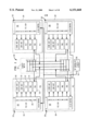
- the 2 ⁇ 2 ManArray 100 further includes a sequence processor (SP) controller 102 which dispatches 32-bit instructions to the array PEs over a single 32-bit bus.
- SP sequence processor
- One type of 32-bit instruction is an execute iVLIW (XV) instruction which contains a VIM address offset value that is used in conjunction with a VIM base address to generate a pointer to the iVLIW which is desired to be executed.
- the PEs 104 are interconnected by a cluster switch 107.
- the SP 102 and each PE 104 in the ManArray architecture as adapted for use in accordance with the present invention contains a quantity of iVLIW memory (VIM) 106 as shown in FIG. 1.
- VIP iVLIW memory
- Each VIM 106 contains storage space to hold multiple VLIW Instruction Addresses 103, and each Address is capable of storing up to eight simplex instructions.
- Presently preferred implementations allow each iVLIW instruction to contain up to five simplex instructions: one associated with each of the Store Unit 108, Load Unit 110, Arithmetic Logic Unit 112 (ALU), Multiply-Accumulate Unit 114 (MAU), and Data-Select Unit 116 (DSU) 116.
- ALU Arithmetic Logic Unit 112
- MAU Multiply-Accumulate Unit
- DSU Data-Select Unit 116
- an iVLIW instruction at VIM address "i" 105 contains the five instructions SLAMD.
- FIG. 2 shows a basic iVLIW data path arrangement 200 by which a fetched instruction is stored in an Instruction Register 20 which is connected to the VIM Load and Store Control function 22.
- the VIM Load and Store Control function provides the interface signals to VIM 24.
- the VIM 24 corresponds to VIM 106, with each VIM 106 of FIG. 1 having associated registers and controls, such as those shown in FIG. 2.
- the output of the VIM 24 is pipelined to the iVLIW register 26.
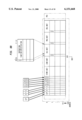
- FIG. 3 illustrates a Five Slot iVLIW VIM 300 with N entries, 0,1 . . . N-1.
- Each VIM 300 addressed location includes storage space for Store, Load, ALU, MAU and DSU instructions 301-305.
- An expanded ALU slot view 303' shows a 32-bit storage space with bit-31 "d” highlighted. The use of the instruction bits in VIM storage will be discussed in greater detail below.
- iVLIW instructions can be loaded into an array of PE VIMs collectively, or, by using special instructions to mask a PE or PEs, each PE VIM can be loaded individually.
- the iVLIW instructions in VIM are accessed for execution through the Execute VLIW (XV) instruction, which, when executed as a single instruction, causes the simultaneous execution of the simplex instructions located at the VIM memory address.
- An XV instruction can cause the simultaneous execution of:
- the LV instruction 400 shown in FIG. 4A is for 32 bit encoding as shown in encoding block 410 and has the presently preferred syntax/operation shown in syntax/operation block 420 as described further below.
- the LV instruction 400 is used to load and/or disable individual instruction slots of the specified SP or PE VLIW Memory (VIM).
- VIM address is computed as the sum of a base VIM address register Vb (V0 or V1) plus an unsigned 8-bit offset VIMOFFS shown in bits 0-7, the block of bits 411, of encoding block 410 in FIG. 4A.
- the VIM address must be in the valid range for the hardware configuration otherwise the operation of this instruction in undefined.
- S Store Unit (SU)
- L Load Unit (LU)
- ALU Arimetic Logic Unit
- MAU Multiply-Accumulate Unit
- DSU Data Select Unit
- the number of instructions to load are specified utilizing an InstrCnt parameter. For the present implementation, valid values are 0-5.
- the next InstrCnt instructions following LV are loaded into the specified VIM.
- the XV instruction 425 shown in FIG. 4B is also for 32 bit encoding as shown in encoding block 430 and has the presently preferred syntax/operation shown in syntax/operation block 435 as described further below.
- the XV instruction 425 is used to execute individual instruction slots of the specified SP or PE VLIW Memory (VIM).
- VIM address is computed as the sum of a base VIM address register Vb (V0 or V1) plus an unsigned 8-bit offset VIMOFFS shown in bits 0-7, the block of bits 431, of encoding block 430 of FIG. 4B.
- the VIM address must be in the valid range for the hardware configuration otherwise the operation of this instruction is undefined.
- the override does not affect the UAF setting specified by the LV instruction.
- FIGS. 4E and 4F illustrate a presently preferred ADD instruction and slot storage for three synchronous MIMD iVLIWs in a 2 ⁇ 2 ManArray configuration, respectively.
- the ADD instruction 450 shown in FIG. 4E is again for 32 bit encoding as shown in encoding block 455 and has the presently preferred syntax/operation shown in syntax/operation block 460 as described further below.
- ADD instruction 450 is used to store the sum of source registers R x and R y in target register R t .
- the v bit is meaningful for signed operations, and the C bit is meaningful for unsigned operations.
- the number of cycles is one.
- the LV and XV instructions may be used to load, modify, disable, or execute iVLIW instructions in individual PEs or PE groups defined by the programmer. To do this, individual PEs are enabled or disabled by an instruction which modifies a Control Register located in each PE which, among other things, enables or disables each PE. To load and operate an individual PE or a group of PEs, the control registers are modified to enable individual PE(s), and to disable all others. Normal iVLIW instructions will then operate only on PEs that are enabled.
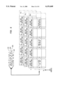
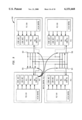
- FIG. 5 shows a selection mechanism for allowing selection of instructions out of VIM memory.
- a fetched instruction is loaded into a first instruction register (IR1) 510.
- Register 510 corresponds generally with instruction register 20 of FIG. 2.
- the output of IR1 is pre-decoded in predecoder or precode function 512 early in the pipeline cycle prior to loading the second instruction register (IR2) 514.
- the pre-decoder 512 When the instruction in IR1 is a Load iVLIW instruction (LV) with a non-zero instruction count, the pre-decoder 512 generates an LVc1 control signal 515, which is used to set up the LV operation cycle, and the VIM address 511 is calculated by use of the specified Vb register 502 added by an adder 504 to an offset value included in the LV instruction via path 503. The resulting VIM address 511 is stored in register 506 and passed through multiplexer 508 to address the VIM 516. VIM 516 corresponds generally to VIM 106 of FIG. 1. Register 506 is required to hold the VIM address 507 during the LV operations.
- LV Load iVLIW instruction
- the VIM address 511 and LV control state allow the loading of the instructions received after the LV instruction into the VIM 516.
- the disable bits 10-17 shown in FIG. 4A, are loaded into the d-bits register 518 for use when loading instructions into the VIM 516.
- the appropriate control signal is generated depending upon the instruction type, Storec1 519, Loadc1 521, ALUc1 523, MAUc1 525, or DSUc1 527.
- the pre-decode function 512 is preferably provided based upon a simple decoding of the Group bits (bits 30 and 31) which define the instruction type shown in FIGS. 4A, B and E and the Unit field bits (bits 27 and 28 which specify the execution unit type) shown in FIGS. 4D and 4E.
- the instruction in IR1 510 can be loaded into VIM 516 in the proper functional unit position.
- the pre-decode function 512 included in the LV list of instructions, when this instruction is received into IR1 510 it can be determined by the pre-decode function 512 that this instruction should be loaded into the ALU Instruction slot 520 in VIM 516.
- the appropriate d-bit 531 for that functional slot position is loaded into bit-31 of that slot.
- the loaded d-bit occupies one of the group code bit positions from the original instruction.
- VIM address 511 Upon receipt of an XV instruction in IR1 510, the VIM address 511 is calculated by use of the specified Vb register 502 added by adder 504 to the offset value included in the XV instruction via path 503. The resulting VIM Address 507 is passed through multiplexer 508 to address the VIM. The iVLIW at the specified address is read out of the VIM 516 and passes through the multiplexers 530, 532, 534, 536, and 538, to the IR2 registers 514. As an alternative to minimize the read VIM access timing critical path, the output of VIM 516 can be latched into a register whose output is passed through a multiplexer prior to the decode state logic.
- the IR2MUX1 control signal 533 in conjunction with the pre-decode XVc1 control signal 517 cause all the IR2 multiplexers, 530, 532, 534, 536, and 538, to select the VIM output paths, 541, 543, 545, 547, and 549.
- the five individual decode and execution stages of the pipeline, 540, 542, 544, 546, and 548, are completed in synchrony providing the iVLIW parallel execution performance.
- the bypass VIM path 535 is shown.
- the pre-decode function 512 when a simplex ADD instruction is received into IR1 510 for parallel array execution, the pre-decode function 512 generates the IR2MUX1 533 control signal, which in conjunction with the instruction type pre-decode signal, 523 in the case of an ADD, and lack of an XV 517 or LV 515 active control signal, causes the ALU multiplexer 534 to select the bypass path 535.
- FIG. 6 shows an exemplary SIMD iVLIW usage of an iVLIW system such as the system 500 shown in FIG. 5.
- FIG. 6 there are J+1 PEs as indicated by the PE numbering PE0 to PEJ.
- a portion of LV code is shown in FIG. 6 indicating that three instructions are to be loaded at VIM address 27 with the Load Unit and MAU instruction slots being disabled.
- This loading operation is determined from the LV instruction 601 based upon the syntax shown in FIG. 4A. Assuming all PEs are masked on, then the indicated three instructions 603, 605, and 607, will be loaded at VIM address 27 in each of the J+1 PEs in the array.
- the result of this loading is indicated in FIG. 6 by showing the instructions stored in their appropriate execution slot in the VIMs, instruction 603 in the ALU slot, instruction 605 in the DSU slot, and instruction 607 in the Store Unit slot.
- the pre-decode function allows the multiple bit-31 positions of the VIM slot fields to be written with the stored d-bits 518 shown in FIG. 5, that were generated from the LV instruction that initiated the VIM loading sequence. It is further noted that the unit field, bits 27 and 28, in the arithmetic instructions, see, for example, FIG. 4E, is needed to determine which VIM slot an arithmetic instruction is to be loaded into.
- VIM 700 in FIG. 7, wherein one of the instruction group bits, bit 30 of FIG. 4E, and the instruction Unit field bits, bits 27 and 28 are replaced in VIM 700 by the Translation Extension Option bits "o" for Opcode Extensions bit-30 labeled 721 of FIG. 7, "r” for Register File Extensions bit-28 labeled 723, and "c” for Conditional Execution Extensions bit-27 labeled 725.
- These additional bits are separately stored in a miscellaneous register 850 shown in FIG. 8A, that the programmer can load to or store from. These bits provide extended capabilities that could not be provided due to lack of instruction encoding bits in a 32-bit instruction format.
- opcode extension bit "o” it is possible to map one set of instructions into a new set of instructions.
- register extension bit "r” it is possible to double the register file space and have two banks of registers providing either additional register space or to act as a fast context switching mechanism allowing two register banks to be split between two contexts.
- condition execution extension bit "c” it is possible to specify two different sets of conditions or specify a different conditional execution functionality under programmer control.
- FIG. 8A depicts an iVLIW system 800 which illustrates aspects of the iVLIW translation extension load and fetch pipeline showing the addition of the o,r, and c bits register 850 and the set of pre-decode control signals 815, 817, 819, 821, 823, 825, 827, and 833. It is noted that other uses of these freed up bits are possible. For example, all three bits could be used for register file extension providing either individual control to the three operand instructions or providing up to eight banks of 32 ⁇ 32 registers.
- the bypass VIM path 835 is shown in FIG. 8A.
- the pre-decode function 812 when a simplex ADD instruction is received into IR1 810 for parallel array execution, the pre-decode function 812 generates the IR2MUX2 833 control signal, which in conjunction with the instruction type pre-decode signal, 823 in the case of an ADD, and lack of an XV 817 or LV 815 active control signal, causes the ALU multiplexer 834 to select the bypass path 835.
- bypass operation is to occur during a full stage of the pipeline, it is possible to replace the group bits and the unit field bits in the bypassed instructions as they enter the IR2 latch stage. This is indicated in FIG. 8A by the "o, r, and c" bits signal path 851 being used to replace the appropriate bit positions at the input to the multiplexers 830, 832, 834, 836, and 838.
- FIG. 8B depicts an alternative form VIM 800' from that shown in FIGS. 7 and 8A.
- the d-bits per execution slot are grouped together with the additional bits "o, r, c and uaf" bits. These ten bits are grouped separately from the execution unit function bits defined in bits 0-26,29 per each slot.
- the unit affecting field (uaf) bits 22 and 23 of FIG. 4A from the LV instruction are required to be stored at a single iVLIW VIM address since the "uaf" bits pertain to which arithmetic unit affects the flags at the time of execution.
- sixteen additional load immediate bits can be stored in a separate "constant" register and loaded in a VIM address to extend the Load Unit's capacity to load 32 bits of immediate data.
- the VIM data width must be expanded appropriately.
- the size of the stored iVLIWs is decoupled from being a multiple of the instruction size thereby allowing the stored iVLIW to be greater than or less than the k*32-bits for a k instruction iVLIW, depending upon requirements.
- a problem may be encountered when implementing SMIMD operations when dealing with inter-PE communications.
- the typical SIMD mode of communications specifies all PEs execute the same inter-PE communication instruction.
- This SIMD inter-PE instruction being the same in each PE, requires a common controlling mechanism to ensure compliance with the common operation defined between the PEs.
- a Send Model is used where a single instruction, such as SEND-WEST, is dispatched to all PEs in the array.
- the SIMD inter-PE communication instruction causes a coordinated control of the network interface between the PEs to allow each PE to send data to the PE topologically defined by the inter-PE instruction.
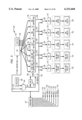
- This single SIMD instruction can be interpreted and the network interface 911 can be controlled by a single PE as shown in FIG. 9 since all PEs receive the same instruction.
- the ManArray 2 ⁇ 2 cluster switch shown in FIG. 9, is made up of four 4-to-1 multiplexers 920, 922, 924, and 926, for the interface Input/Output (I/O) buses between the DSU. These buses can be 8, 9, 16, 32, 64, or other number of bit, bit buses without restriction.
- the control of a single 4-to-1 multiplexer requires only two bits of control to select one out of four of the possible paths.
- SIMD SIMD
- FIG. 10 a centralized controller 1010 receives the same dispatched inter-PE communication instruction 1011 from the SP controller as do the other PEs in the network. This mechanism allows the network connections to be changed on a cycle-by-cycle basis.
- Two attributes of the SIMD Send Model are a common instruction to all PEs and the specification of both sender and receiver. In the SIMD mode, this approach is not a problem.
- a Receive Model is advantageously employed.
- the single point of network control be it located in a single PE or in a centralized control mechanism, that is facilitated by the Send Model is replaced in the Receive Model with distributed network interface control.
- Each PE controls its own receive port.
- the Receive Model specifies the receive path through the network interface. In the case of the ManArray network, each PE controls its own multiplexer input path of the cluster switch.
- each PE has its own control of its input multiplexer, 1120, 1122, 1124 or 1126, respectively.
- PE0 has control signals 1111 for controlling its input multiplexer 1120.
- the Receive Model also requires that data be made available on the PEs output port to the interface network without target PE specification. Consequently, for any meaningful communication to occur between processing elements using the Receive Model, the PEs must be programmed to cooperate in the receiving of the data that is made available. Using Synchronous MIMD, this cooperation is guaranteed to occur if the cooperating instructions exist in the same iVLIW location.
- the cooperating PEs execute the proper inter-PE communications instructions to cause data movement between any two or more PEs.
- a group can vary in size from two PEs to the whole array of PEs. While FIG. 11 does not show an SP, such as the SP controller 102 of FIG. 1, for ease and clarity of illustration, such a controller will preferably be included although it will be recognized that SP functionality can be merged with a PE such as PEO as taught in U.S. Provisional Application Ser. No. 60/077,457 previously incorporated by reference, or SP functionality could be added to all of the PEs although such increased functionality would be relatively costly.
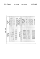
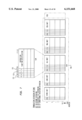
- FIG. 4F shows the definition 470 of three Synchronous-MIMD iVLIWs in a 2 ⁇ 2 ManArray configuration.
- the top section 480 gives a descriptive view of the operations.
- the bottom section 490 gives the corresponding instruction mnemonics which are loaded in the LU, MAU, ALU, DSU and SU, respectively.
- Each iVLIW contains four rows between thick black lines, one for each PE.
- the leftmost column of the figure shows the address where the iVLIW is loaded in PE iVLIW Instruction Memory (VIM).
- VIP PE iVLIW Instruction Memory
- the next column shows the PE number.
- Each iVLIW contains one row for each PE, showing the instructions which are loaded into that PE's VIM entry.
- the remaining columns list the instruction for each of the five execution units: Load Unit (LU), Multiply-Accumulate Unit (MAU), Arithmetic Logic Unit (ALU), Data Select Unit (DSU), and Store Unit (SU).
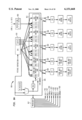
- VIM entry number 29 in PE2 495 is loaded with the four instructions li.p.w R3, A1+, A7, fmpy.pm.1fw R5, R2, R31, fadd.pa.1fw R9, R7, R5, and pexchg.pd.w R8, R0 2 ⁇ 2 -- PE3. These instructions are those found in the next to last row of FIG. 4F. That same VIM entry (29) contains different instructions in PEs 0, 1, and 3, as can be seen by the rows corresponding to these PEs on VIM entry 29, for PE0 491, PE2 493, and PE3 497.
- the following example 1--1 shows the sequence of instructions which load the PE VIM memories as defined in FIG. 4F. Note that PE Masking is used in order to load different instructions into different PE VIMs at the same address.
- the following example 1-2 shows the sequence of instructions which execute the PE VIM entries as loaded by the example 1--1 code in FIG. 4F. Note that no PE Masking is necessary.
- the specified VIM entry is executed in each of the PEs, PE0, PE1, PE2, and PE3.
- the iVLIWs defined in FIG. 4F are used to effect the dot product of a constant 3 ⁇ 1 vector with a stream of variable 3 ⁇ 1 vectors stored in PE local data memories.
- Each PE stores one element of the vector.
- PE1 stores the x component
- PE2 stores the y component
- PE3 stores the z component.
- PE0 stores no component.
- the constant vector is held in identical fashion in a PE register, in this case, compute register R31.
- the iVLIWs operate on three variable vectors at a time. Due to the distribution of the vector components over the PEs, it is not feasible to use PEO to compute a 4 th vector dot product. PEO is advantageously employed instead to take care of some setup for a future algorithm stage. This can be seen in the iVLIW load slots, as vector 1 is loaded in iVLIW 27 (component-wise across the PEs, as described above), vector 2 is loaded in iVLIW 28, and vector 3 is loaded in iVLIW 29 (li.p.w R*, A1+, A7). PE1 computes the x component of the dot product for each of the three vectors.
- PE2 computes the y component
- PE3 computes the z component (fmpy.pm.1fw R*, R*, R31).
- communication among the PEs must occur in order to get the y and z components of the vector 1 dot product to PE1, the x and z components of the vector 2 dot product to PE2, and the x and y components of the vector 3 dot product to PE3.
- This communication occurs in the DSU via the pexchg instruction.
- each PE is summing (fadd.pa.1fw R9, R7, R* and fadd.pa.1fw R10, R9, R8) the components of a unique dot product result simultaneously.
- These results are then stored (si.p.w R10, +A2, A6) into PE memories. Note that each PE will compute and store every third result. The final set of results are then accessed in round-robin fashion from PEs 1, 2, and 3.
- each PE performs a comparison (fcmpLE.pa.1fw R10, R0) of its dot product result with zero (held in PE register R0), and conditionally stores a zero (t.sii.p.w R0, A2+, 0) in place of the computed dot product if that dot product was negative. In other words, it is determined if the comparison is R10 less than R0? is true.
- This implementation of a dot product with removal of negative values is used, for example, in lighting calculations for 3D graphics applications.
- the present invention has been disclosed in the context of presently preferred methods and apparatus for carrying out the invention, various alternative implementations and variations will be readily apparent to those of ordinary skill in the art.
- the present invention does not preclude the ability to load an instruction into VIM and also execute the instruction. This capability was deemed an unnecessary complication for the presently preferred programming model among other considerations such as instruction formats and hardware complexity. Consequently, the Load iVLIW delimiter approach was chosen.
Abstract
Description
__________________________________________________________________________
! first load in instructions common to PEs 1,2,3
lim.s.h0 SCR1, 1 ! mask off PE0 in order to load in 1,2,3
  lim.s.h0 VAR, 0 ! load VIM base address reg v0 with zero
  lv.p v0, 27, 2, d=, f= ! load VIM entry v0 + 27 (=27) with the
   ! next two instructions; disable no
   ! instrs; default flag setting to ALU
li.p.w R1, A1+, A7 ! load instruction into LU
  fmpy.pm.1fw R6, R3, R31 ! mpy instruction into MAU
lv.p v0, 28, 2, d=, f=
                 ! load VIM entry v0 + 28 (=28) with the
   ! next two instructions; disable no
   ! instrs; default flag setting to ALU
li.p.w R2, A1+, A7 ! load instruction into LU
  fmpy.pm.1fw R4, R1, R31 ! mpy instruction into MAU
lv.p v0, 29, 2, d=, f=
                 ! load VIM entry v0 + 29 (=29) with the
   ! next two instructions; disable no
   ! instrs; default flag setting to ALU
li.p.w R3, A1+, A7 ! load instruction into LU
  fmpy.pm.1fw R5, R2, R31 ! mpy instruction into MAU
! now load in instructions unique to PE0
lim.s.h0 SCR1, 14
                 ! mask off PEs 1,2,3 to load PE0
  nop ! one cycle delay to set mask
  lv.p v0, 27, 1, d = lmad, f= ! load VIM entry v0 + 27 (=27) with the
                   ! next instruction; disable instrs
   ! in LU, MAU, ALU, DSU slots; default
   ! flag setting to ALU
si.p.w R1, A2+, R28
                   ! store instruction into SU
lv.p v0, 28, 1, d = lmad, f=
                 ! load VIM entry v0 + 28 (=28) with the
   ! next instruction; disable instrs
   ! in LU, MAU, ALU, DSU slots; default
   ! flag setting to ALU
si.p.w R1, A2+, R28
                   ! store instruction into SU
lv.p v0, 29, 1, d = lmad, f=
                 ! load VIM entry v0 + 29 (=29) with the
   ! next instruction; disable instrs
   ! in LU, MAU, ALU, DSU slots; default
   ! flag setting to ALU
si.p.w R1, A2+, R28
                   ! store instruction into SU
! now load in instructions unique to PE1
lim.s.h0 SCR1, 13
                 ! mask off PEs 0,2,3 to load PE1
  nop ! one cycle delay to set mask
  lv.p v0, 27, 3, d=, f= ! load VIM entry v0 + 27 (=27) with the
   ! next three instructions; disable no
   ! instrs; default flag setting to ALU
fadd.pa.1fw R10, R9, R8
                   ! add instruction into ALU
pexchg.pd.w R7, R0, 2 × 2.sub.-- PE3
                 ! pe comm instruction into DSU
si.p.w R10, +A2, A6
                   ! store instruction into SU
lv.p v0, 28, 2, d = s, f=
                 ! load VIM entry v0 + 28 (=28) with the
   ! next two instructions; disable instr
   ! in SU slot; default flag setting to ALU
fadd.pa.1fw R9, R7, R4
                   ! add instruction into ALU
pexchg.pd.w R8, R5, 2 × 2.sub.-- PE2
                 ! pe comm instruction into DSU
lv.p v0, 29, 3, d=, f=
                 ! load VIM entry v0 + 29 (=29) with the
   ! next three instructions; disable no
   ! instrs; default flag setting to ALU
fcmpLE.pa.1fw R10, R0
                   ! compare instruction into ALU
pexchg.pd.w R15, R6, 2 × 2.sub.-- PE1
                 ! pe comm instruction into DSU
t.sii.p.w R0, A2+, 0
                   ! store instruction into SU
! now load in instructions unique to PE2
lim.s.h0 SCR1, 11
                 ! mask off PEs 0,1,3 to load PE2
  nop ! one cycle delay to set mask
  lv.p v0, 27, 3, d=, f= ! load VIM entry v0 + 27 (=27) with the
   ! next three instructions; disable no
   ! instrs; default flag setting to ALU
fcmpLE.pa.1fw R10, R0
                   ! compare instruction into ALU
pexchg.pd.w R15, R6, 2 × 2.sub.-- PE2
                 ! pe comm instruction into DSU
t.sii.p.w R0, A2+, 0
                   ! store instruction into SU
lv.p v0, 28, 3, d=, f=
                 ! load VIM entry v0 + 28 (=28) with the
   ! next three instructions; disable no
   ! instrs; default flag setting to ALU
fadd.pa.1fw R10, R9, R8
                   ! add instruction into ALU
pexchg.pd.w R7, R4, 2 × 2.sub.-- PE1
                 ! pe comm instruction into DSU
si.p.w R10, +A2, A6
                   ! store instruction into SU
lv.p v0, 29, 2, d = s, f=
                 ! load VIM entry v0 + 29 (=29) with the
   ! next two instructions; disable instr
   ! in SU slot; default flag setting to ALU
fadd.pa.1fw R9, R7, R5
                   ! add instruction into ALU
pexchg.pd.w R8, R0, 2 × 2.sub.-- PE3
                 ! pe comm instruction into DSU
! now load in instructions unique to PE3
lim.s.h0 SCR1, 7 ! mask off PEs 0,1,2 to load PE3
  nop ! one cycle delay to set mask
  lv.p v0, 27, 2, d = s, f= ! load VIM entry v0 + 27 (=27) with the
                   ! next two instructions; disable instr
   ! in SU slot; default flag setting to ALU
fadd.pa.1fw R9, R7, R6
                   ! add instruction into ALU
pexchg.pd.w R8, R4, 2 × 2.sub.-- PE2
                 ! pe comm instruction into DSU
lv.p v0, 28, 2, d = d, f=
                 ! load VIM entry v0 + 28 (=28) with the
   ! next 2 instructions; disable instr in
   ! DSU slot; default flag setting to ALU
fcmpLE.pa.1fw R10, R0
                   ! compare instruction into ALU
  t.sii.p.w R0, A2+, 0 ! store instruction into SU
lv.p v0, 29, 3, d=, f=
                 ! load VIM entry v0 + 29 (=29) with the
   ! next three instructions; disable no
   ! instrs; default flag setting to ALU
fadd.pa.1fw R10, R9, R8
                   ! add instruction into ALU
pexchg.pd.w R7, R5, 2 × 2.sub.-- PE1
                 ! pe comm instruction into DSU
si.p.w R10, +A2, A6
                   ! store instruction into SU
lim.s.h0 SCR1, 0 ! reset PE mask so all PEs are on
  nop ! one cycle delay to set mask
__________________________________________________________________________
__________________________________________________________________________
! address register, loop, and other setup would be here
  ....
  ! startup VLIW execution
  ! f = parameter indicates default to LV flag setting
xv.p v0, 27, e = l, f=
            ! execute VIM entry V0 + 27, LU only
  xv.p v0, 28, e = lm, f=  ! execute VIM entry V0 + 28, LU, MAU only
             xv.p v0, 29, e = lm, f=  ! execute VIM entry V0 + 29, LU,
            MAU only
  xv.p v0, 27, e = lmd, f=   ! execute VIM entry V0 + 27, LU, MAU, DSU
            only
  xv.p v0, 28, e = lamd, f=    ! execute VIM entry V0 + 28, all units
            except SU
  xv.p v0, 29, e = lamd, f=    ! execute VIM entry V0 + 29, all units
            except SU
  xv.p v0, 27, e = lamd, f=    ! execute VIM entry V0 + 27, all units
            except SU
  xv.p v0, 28, e = lamd, f=    ! execute VIM entry V0 + 28, all units
            except SU
  xv.p v0, 29, e = lamd, f=    ! execute VIM entry V0 + 29, all units
            except SU
! loop body - mechanism to enable looping has been previously set up
loop.sub.-- begin: xv.p v0, 27, e = slamd, f=
                   ! execute v0 + 27, all units
xv.p v0, 28, e = slamd, f=
                   ! execute v0 + 28, all units
loop.sub.-- end: xv.p v0, 29, e = slamd, f=
                   ! execute v0 + 29, all units
__________________________________________________________________________
Claims (41)
Priority Applications (3)
| Application Number | Priority Date | Filing Date | Title |
|---|---|---|---|
| US09/187,539 US6151668A (en) | 1997-11-07 | 1998-11-06 | Methods and apparatus for efficient synchronous MIMD operations with iVLIW PE-to-PE communication |
| US09/677,732 US6446191B1 (en) | 1997-11-07 | 2000-10-02 | Methods and apparatus for efficient synchronous MIMD operations with iVLIW PE-to-PE communication |
| US10/872,995 USRE41703E1 (en) | 1997-11-07 | 2004-06-21 | Methods and apparatus for efficient synchronous MIMD operations with IVLIW PE-TO-PE communication |
Applications Claiming Priority (2)
| Application Number | Priority Date | Filing Date | Title |
|---|---|---|---|
| US6461997P | 1997-11-07 | 1997-11-07 | |
| US09/187,539 US6151668A (en) | 1997-11-07 | 1998-11-06 | Methods and apparatus for efficient synchronous MIMD operations with iVLIW PE-to-PE communication |
Related Child Applications (1)
| Application Number | Title | Priority Date | Filing Date |
|---|---|---|---|
| US09/677,732 Continuation US6446191B1 (en) | 1997-11-07 | 2000-10-02 | Methods and apparatus for efficient synchronous MIMD operations with iVLIW PE-to-PE communication |
Publications (1)
| Publication Number | Publication Date |
|---|---|
| US6151668A true US6151668A (en) | 2000-11-21 |
Family
ID=22057176
Family Applications (3)
| Application Number | Title | Priority Date | Filing Date |
|---|---|---|---|
| US09/187,539 Expired - Lifetime US6151668A (en) | 1997-11-07 | 1998-11-06 | Methods and apparatus for efficient synchronous MIMD operations with iVLIW PE-to-PE communication |
| US09/677,732 Ceased US6446191B1 (en) | 1997-11-07 | 2000-10-02 | Methods and apparatus for efficient synchronous MIMD operations with iVLIW PE-to-PE communication |
| US10/872,995 Expired - Lifetime USRE41703E1 (en) | 1997-11-07 | 2004-06-21 | Methods and apparatus for efficient synchronous MIMD operations with IVLIW PE-TO-PE communication |
Family Applications After (2)
| Application Number | Title | Priority Date | Filing Date |
|---|---|---|---|
| US09/677,732 Ceased US6446191B1 (en) | 1997-11-07 | 2000-10-02 | Methods and apparatus for efficient synchronous MIMD operations with iVLIW PE-to-PE communication |
| US10/872,995 Expired - Lifetime USRE41703E1 (en) | 1997-11-07 | 2004-06-21 | Methods and apparatus for efficient synchronous MIMD operations with IVLIW PE-TO-PE communication |
Country Status (10)
| Country | Link |
|---|---|
| US (3) | US6151668A (en) |
| EP (1) | EP1029266B1 (en) |
| JP (1) | JP4156794B2 (en) |
| KR (1) | KR20010031884A (en) |
| CN (1) | CN100380313C (en) |
| AT (1) | ATE362623T1 (en) |
| CA (1) | CA2310584A1 (en) |
| DE (1) | DE69837791T2 (en) |
| IL (1) | IL135953A0 (en) |
| WO (1) | WO1999024903A1 (en) |
Cited By (57)
| Publication number | Priority date | Publication date | Assignee | Title |
|---|---|---|---|---|
| US20010037471A1 (en) * | 2000-03-01 | 2001-11-01 | Ming-Kang Liu | System and method for internal operation of multiple-port xDSL communications systems |
| US6356994B1 (en) * | 1998-07-09 | 2002-03-12 | Bops, Incorporated | Methods and apparatus for instruction addressing in indirect VLIW processors |
| US20020120830A1 (en) * | 2001-02-23 | 2002-08-29 | Masahito Matsuo | Data processor assigning the same operation code to multiple operations |
| US20030039574A1 (en) * | 2000-04-25 | 2003-02-27 | Bannykh Oleg Alexandrovich | Austenitic steel |
| US20030163669A1 (en) * | 2002-02-27 | 2003-08-28 | Eric Delano | Configuration of multi-cluster processor from single wide thread to two half-width threads |
| US20040148488A1 (en) * | 1998-03-10 | 2004-07-29 | Pts Corporation | Merged array controller with processing element |
| US6785800B1 (en) * | 1999-09-10 | 2004-08-31 | Ricoh Company, Ltd. | Single instruction stream multiple data stream processor |
| US6839728B2 (en) * | 1998-10-09 | 2005-01-04 | Pts Corporation | Efficient complex multiplication and fast fourier transform (FFT) implementation on the manarray architecture |
| US20050216700A1 (en) * | 2004-03-26 | 2005-09-29 | Hooman Honary | Reconfigurable parallelism architecture |
| US20060224865A1 (en) * | 2001-10-31 | 2006-10-05 | Stephen Barlow | Vector processing system |
| US20070204137A1 (en) * | 2004-08-30 | 2007-08-30 | Texas Instruments Incorporated | Multi-threading processors, integrated circuit devices, systems, and processes of operation and manufacture |
| US20070250688A1 (en) * | 2004-11-05 | 2007-10-25 | Nec Corporation | Simd Type Parallel Arithmetic Device, Processing Element and Control System of Simd Type Parallel Arithmetic Device |
| US20080082800A1 (en) * | 2002-07-19 | 2008-04-03 | Renesas Technology Corp. | Data processor for modifying and executing operation of instruction code |
| US20080120489A1 (en) * | 2006-11-16 | 2008-05-22 | Shinri Inamori | Scalable Multi-Threaded Sequencing/Synchronizing Processor Architecture |
| US7401204B1 (en) * | 1999-10-01 | 2008-07-15 | Fujitsu Limited | Parallel Processor efficiently executing variable instruction word |
| US20080209437A1 (en) * | 2006-08-17 | 2008-08-28 | International Business Machines Corporation | Multithreaded multicore uniprocessor and a heterogeneous multiprocessor incorporating the same |
| US20080301413A1 (en) * | 2006-08-23 | 2008-12-04 | Xiaolin Wang | Method of and apparatus and architecture for real time signal processing by switch-controlled programmable processor configuring and flexible pipeline and parallel processing |
| US7493474B1 (en) * | 2004-11-10 | 2009-02-17 | Altera Corporation | Methods and apparatus for transforming, loading, and executing super-set instructions |
| US20090125574A1 (en) * | 2007-11-12 | 2009-05-14 | Mejdrich Eric O | Software Pipelining On a Network On Chip |
| US20090157976A1 (en) * | 2007-12-13 | 2009-06-18 | Miguel Comparan | Network on Chip That Maintains Cache Coherency With Invalidate Commands |
| US20090187716A1 (en) * | 2008-01-17 | 2009-07-23 | Miguel Comparan | Network On Chip that Maintains Cache Coherency with Invalidate Commands |
| US20090201302A1 (en) * | 2008-02-12 | 2009-08-13 | International Business Machines Corporation | Graphics Rendering On A Network On Chip |
| US20090210592A1 (en) * | 2008-02-15 | 2009-08-20 | International Business Machines Corporation | Network On Chip With A Low Latency, High Bandwidth Application Messaging Interconnect |
| US20090228684A1 (en) * | 2008-03-05 | 2009-09-10 | The Boeing Company | Intelligent Fabric System on a Chip |
| US20090245257A1 (en) * | 2008-04-01 | 2009-10-01 | International Business Machines Corporation | Network On Chip |
| US20090271172A1 (en) * | 2008-04-24 | 2009-10-29 | International Business Machines Corporation | Emulating A Computer Run Time Environment |
| US20090271597A1 (en) * | 2008-04-24 | 2009-10-29 | International Business Machines Corporations | Branch Prediction In A Computer Processor |
| US20090282214A1 (en) * | 2008-05-09 | 2009-11-12 | International Business Machines Corporation | Network On Chip With Low Latency, High Bandwidth Application Messaging Interconnects That Abstract Hardware Inter-Thread Data Communications Into An Architected State of A Processor |
| US20090282222A1 (en) * | 2008-05-09 | 2009-11-12 | International Business Machines Corporation | Dynamic Virtual Software Pipelining On A Network On Chip |
| US20090282227A1 (en) * | 2008-05-09 | 2009-11-12 | International Business Machines Corporation | Monitoring Software Pipeline Performance On A Network On Chip |
| US20090282221A1 (en) * | 2008-05-09 | 2009-11-12 | International Business Machines Corporation | Preferential Dispatching Of Computer Program Instructions |
| US20090285222A1 (en) * | 2008-05-15 | 2009-11-19 | International Business Machines Corporation | Network On Chip With Minimum Guaranteed Bandwidth For Virtual Communications Channels |
| US20090300336A1 (en) * | 2008-05-29 | 2009-12-03 | Axis Semiconductor, Inc. | Microprocessor with highly configurable pipeline and executional unit internal hierarchal structures, optimizable for different types of computational functions |
| US20090300337A1 (en) * | 2008-05-29 | 2009-12-03 | Axis Semiconductor, Inc. | Instruction set design, control and communication in programmable microprocessor cases and the like |
| US7634637B1 (en) * | 2005-12-16 | 2009-12-15 | Nvidia Corporation | Execution of parallel groups of threads with per-instruction serialization |
| US20100070714A1 (en) * | 2008-09-18 | 2010-03-18 | International Business Machines Corporation | Network On Chip With Caching Restrictions For Pages Of Computer Memory |
| US7743235B2 (en) * | 2000-08-31 | 2010-06-22 | Intel Corporation | Processor having a dedicated hash unit integrated within |
| US7991983B2 (en) | 1999-09-01 | 2011-08-02 | Intel Corporation | Register set used in multithreaded parallel processor architecture |
| US8095775B1 (en) * | 2007-11-21 | 2012-01-10 | Marvell International Ltd. | Instruction pointers in very long instruction words |
| US8214845B2 (en) | 2008-05-09 | 2012-07-03 | International Business Machines Corporation | Context switching in a network on chip by thread saving and restoring pointers to memory arrays containing valid message data |
| US8230179B2 (en) | 2008-05-15 | 2012-07-24 | International Business Machines Corporation | Administering non-cacheable memory load instructions |
| US8237705B2 (en) | 2005-12-16 | 2012-08-07 | Nvidia Corporation | Hierarchical processor array |
| US8392664B2 (en) | 2008-05-09 | 2013-03-05 | International Business Machines Corporation | Network on chip |
| US8423715B2 (en) | 2008-05-01 | 2013-04-16 | International Business Machines Corporation | Memory management among levels of cache in a memory hierarchy |
| US8438578B2 (en) | 2008-06-09 | 2013-05-07 | International Business Machines Corporation | Network on chip with an I/O accelerator |
| US8473667B2 (en) | 2008-01-11 | 2013-06-25 | International Business Machines Corporation | Network on chip that maintains cache coherency with invalidation messages |
| US8490110B2 (en) | 2008-02-15 | 2013-07-16 | International Business Machines Corporation | Network on chip with a low latency, high bandwidth application messaging interconnect |
| US8494833B2 (en) | 2008-05-09 | 2013-07-23 | International Business Machines Corporation | Emulating a computer run time environment |
| US8526422B2 (en) | 2007-11-27 | 2013-09-03 | International Business Machines Corporation | Network on chip with partitions |
| US8884920B1 (en) | 2011-05-25 | 2014-11-11 | Marvell International Ltd. | Programmatic sensing of capacitive sensors |
| US9069553B2 (en) | 2011-09-06 | 2015-06-30 | Marvell World Trade Ltd. | Switching tasks between heterogeneous cores |
| US9098694B1 (en) | 2011-07-06 | 2015-08-04 | Marvell International Ltd. | Clone-resistant logic |
| US9304812B2 (en) | 2010-12-16 | 2016-04-05 | Imagination Technologies Limited | Multi-phased and multi-threaded program execution based on SIMD ratio |
| US9354890B1 (en) | 2007-10-23 | 2016-05-31 | Marvell International Ltd. | Call stack structure for enabling execution of code outside of a subroutine and between call stack frames |
| US9442758B1 (en) | 2008-01-21 | 2016-09-13 | Marvell International Ltd. | Dynamic processor core switching |
| US9582443B1 (en) | 2010-02-12 | 2017-02-28 | Marvell International Ltd. | Serial control channel processor for executing time-based instructions |
| US10565036B1 (en) | 2019-02-14 | 2020-02-18 | Axis Semiconductor, Inc. | Method of synchronizing host and coprocessor operations via FIFO communication |
Families Citing this family (16)
| Publication number | Priority date | Publication date | Assignee | Title |
|---|---|---|---|---|
| US6798834B1 (en) | 1996-08-15 | 2004-09-28 | Mitsubishi Denki Kabushiki Kaisha | Image coding apparatus with segment classification and segmentation-type motion prediction circuit |
| US6366999B1 (en) * | 1998-01-28 | 2002-04-02 | Bops, Inc. | Methods and apparatus to support conditional execution in a VLIW-based array processor with subword execution |
| US6826522B1 (en) * | 1999-06-21 | 2004-11-30 | Pts Corporation | Methods and apparatus for improved efficiency in pipeline simulation and emulation |
| US6748517B1 (en) * | 1999-06-22 | 2004-06-08 | Pts Corporation | Constructing database representing manifold array architecture instruction set for use in support tool code creation |
| WO2003084865A2 (en) | 2001-06-14 | 2003-10-16 | Hyperion Catalysis International, Inc. | Field emission devices using modified carbon nanotubes |
| JPWO2003084243A1 (en) | 2002-03-28 | 2005-08-11 | ソニー株式会社 | Image compression encoding apparatus and method, and program |
| CN1732457A (en) * | 2002-12-30 | 2006-02-08 | 皇家飞利浦电子股份有限公司 | Processing system |
| JP2006522399A (en) * | 2003-04-07 | 2006-09-28 | コーニンクレッカ フィリップス エレクトロニクス エヌ ヴィ | Data processing system having clustered ILP processors |
| US7725681B2 (en) * | 2003-08-15 | 2010-05-25 | Nxp B.V. | Parallel processing array |
| US7299339B2 (en) * | 2004-08-30 | 2007-11-20 | The Boeing Company | Super-reconfigurable fabric architecture (SURFA): a multi-FPGA parallel processing architecture for COTS hybrid computing framework |
| KR100636596B1 (en) * | 2004-11-25 | 2006-10-23 | 한국전자통신연구원 | Parallel Data Path Architecture for High Energy Efficient |
| US7912311B2 (en) * | 2005-03-21 | 2011-03-22 | Intel Corporation | Techniques to filter media signals |
| WO2006123822A1 (en) * | 2005-05-20 | 2006-11-23 | Sony Corporation | Signal processor |
| KR100960148B1 (en) * | 2008-05-07 | 2010-05-27 | 한국전자통신연구원 | Data processing circuit |
| JP2010039625A (en) * | 2008-08-01 | 2010-02-18 | Renesas Technology Corp | Parallel arithmetic device |
| WO2011094346A1 (en) * | 2010-01-26 | 2011-08-04 | Hobbs Barry L | Integrated concurrent multi-standard encoder, decoder and transcoder |
Citations (5)
| Publication number | Priority date | Publication date | Assignee | Title |
|---|---|---|---|---|
| US5649135A (en) * | 1995-01-17 | 1997-07-15 | International Business Machines Corporation | Parallel processing system and method using surrogate instructions |
| US5659785A (en) * | 1995-02-10 | 1997-08-19 | International Business Machines Corporation | Array processor communication architecture with broadcast processor instructions |
| US5682491A (en) * | 1994-12-29 | 1997-10-28 | International Business Machines Corporation | Selective processing and routing of results among processors controlled by decoding instructions using mask value derived from instruction tag and processor identifier |
| US6026478A (en) * | 1997-08-01 | 2000-02-15 | Micron Technology, Inc. | Split embedded DRAM processor |
| US6076154A (en) * | 1998-01-16 | 2000-06-13 | U.S. Philips Corporation | VLIW processor has different functional units operating on commands of different widths |
Family Cites Families (8)
| Publication number | Priority date | Publication date | Assignee | Title |
|---|---|---|---|---|
| JPH0740252B2 (en) * | 1986-03-08 | 1995-05-01 | 株式会社日立製作所 | Multi-processor system |
| DE4129614C2 (en) * | 1990-09-07 | 2002-03-21 | Hitachi Ltd | System and method for data processing |
| US5765011A (en) * | 1990-11-13 | 1998-06-09 | International Business Machines Corporation | Parallel processing system having a synchronous SIMD processing with processing elements emulating SIMD operation using individual instruction streams |
| US5963745A (en) * | 1990-11-13 | 1999-10-05 | International Business Machines Corporation | APAP I/O programmable router |
| US6002880A (en) * | 1992-12-29 | 1999-12-14 | Philips Electronics North America Corporation | VLIW processor with less instruction issue slots than functional units |
| US5680597A (en) * | 1995-01-26 | 1997-10-21 | International Business Machines Corporation | System with flexible local control for modifying same instruction partially in different processor of a SIMD computer system to execute dissimilar sequences of instructions |
| US5669001A (en) * | 1995-03-23 | 1997-09-16 | International Business Machines Corporation | Object code compatible representation of very long instruction word programs |
| US5870576A (en) * | 1996-12-16 | 1999-02-09 | Hewlett-Packard Company | Method and apparatus for storing and expanding variable-length program instructions upon detection of a miss condition within an instruction cache containing pointers to compressed instructions for wide instruction word processor architectures |
-
1998
- 1998-11-06 CA CA002310584A patent/CA2310584A1/en not_active Abandoned
- 1998-11-06 WO PCT/US1998/023650 patent/WO1999024903A1/en active IP Right Grant
- 1998-11-06 IL IL13595398A patent/IL135953A0/en unknown
- 1998-11-06 DE DE69837791T patent/DE69837791T2/en not_active Expired - Lifetime
- 1998-11-06 EP EP98957630A patent/EP1029266B1/en not_active Expired - Lifetime
- 1998-11-06 CN CNB988107678A patent/CN100380313C/en not_active Expired - Fee Related
- 1998-11-06 JP JP2000519833A patent/JP4156794B2/en not_active Expired - Fee Related
- 1998-11-06 KR KR1020007004975A patent/KR20010031884A/en not_active Application Discontinuation
- 1998-11-06 US US09/187,539 patent/US6151668A/en not_active Expired - Lifetime
- 1998-11-06 AT AT98957630T patent/ATE362623T1/en not_active IP Right Cessation
-
2000
- 2000-10-02 US US09/677,732 patent/US6446191B1/en not_active Ceased
-
2004
- 2004-06-21 US US10/872,995 patent/USRE41703E1/en not_active Expired - Lifetime
Patent Citations (5)
| Publication number | Priority date | Publication date | Assignee | Title |
|---|---|---|---|---|
| US5682491A (en) * | 1994-12-29 | 1997-10-28 | International Business Machines Corporation | Selective processing and routing of results among processors controlled by decoding instructions using mask value derived from instruction tag and processor identifier |
| US5649135A (en) * | 1995-01-17 | 1997-07-15 | International Business Machines Corporation | Parallel processing system and method using surrogate instructions |
| US5659785A (en) * | 1995-02-10 | 1997-08-19 | International Business Machines Corporation | Array processor communication architecture with broadcast processor instructions |
| US6026478A (en) * | 1997-08-01 | 2000-02-15 | Micron Technology, Inc. | Split embedded DRAM processor |
| US6076154A (en) * | 1998-01-16 | 2000-06-13 | U.S. Philips Corporation | VLIW processor has different functional units operating on commands of different widths |
Non-Patent Citations (8)
| Title |
|---|
| G.D. Jones and L.D. Larsen, "Pre-Composed Superscalar Architecture", IBM Technical Bulletin, vol. 37, No. 09, Sep. 1994, pp. 447-451. |
| G.D. Jones and L.D. Larsen, "Selecting Predecoded Instructions with a Surrogate", IBM Technical Disclosure Bulletin, vol. 36, No. 06A, Jun. 1993, pp. 35-37. |
| G.D. Jones and L.D. Larsen, Pre Composed Superscalar Architecture , IBM Technical Bulletin, vol. 37, No. 09, Sep. 1994, pp. 447 451. * |
| G.D. Jones and L.D. Larsen, Selecting Predecoded Instructions with a Surrogate , IBM Technical Disclosure Bulletin, vol. 36, No. 06A, Jun. 1993, pp. 35 37. * |
| Johnson, John D., Expansion Caches for Superscalar Processors, Stanford University, Jun. 1994, pp. 1 8. * |
| Johnson, John D., Expansion Caches for Superscalar Processors, Stanford University, Jun. 1994, pp. 1-8. |
| Managawa et al, Pre Decoding Mechanism for Superscalar Architecture, IEEE, May 1991, pp. 1 8. * |
| Managawa et al, Pre-Decoding Mechanism for Superscalar Architecture, IEEE, May 1991, pp. 1-8. |
Cited By (106)
| Publication number | Priority date | Publication date | Assignee | Title |
|---|---|---|---|---|
| US20040148488A1 (en) * | 1998-03-10 | 2004-07-29 | Pts Corporation | Merged array controller with processing element |
| US6874078B2 (en) * | 1998-03-10 | 2005-03-29 | Pts Corporation | Merged control/process element processor for executing VLIW simplex instructions with SISD control/SIMD process mode bit |
| US6356994B1 (en) * | 1998-07-09 | 2002-03-12 | Bops, Incorporated | Methods and apparatus for instruction addressing in indirect VLIW processors |
| US6581152B2 (en) * | 1998-07-09 | 2003-06-17 | Bops, Inc. | Methods and apparatus for instruction addressing in indirect VLIW processors |
| US6839728B2 (en) * | 1998-10-09 | 2005-01-04 | Pts Corporation | Efficient complex multiplication and fast fourier transform (FFT) implementation on the manarray architecture |
| US7991983B2 (en) | 1999-09-01 | 2011-08-02 | Intel Corporation | Register set used in multithreaded parallel processor architecture |
| US6785800B1 (en) * | 1999-09-10 | 2004-08-31 | Ricoh Company, Ltd. | Single instruction stream multiple data stream processor |
| US7401204B1 (en) * | 1999-10-01 | 2008-07-15 | Fujitsu Limited | Parallel Processor efficiently executing variable instruction word |
| US7200138B2 (en) | 2000-03-01 | 2007-04-03 | Realtek Semiconductor Corporation | Physical medium dependent sub-system with shared resources for multiport xDSL system |
| US7295571B2 (en) | 2000-03-01 | 2007-11-13 | Realtek Semiconductor Corp. | xDSL function ASIC processor and method of operation |
| US20020049581A1 (en) * | 2000-03-01 | 2002-04-25 | Ming-Kang Liu | Physical medium dependent sub-system with shared resources for multiport xDSL system |
| US7818748B2 (en) | 2000-03-01 | 2010-10-19 | Realtek Semiconductor Corporation | Programmable task scheduler |
| US20010049756A1 (en) * | 2000-03-01 | 2001-12-06 | Ming-Kang Liu | Transport convergence sub-system with shared resources for multiport xDSL system |
| US20020010849A1 (en) * | 2000-03-01 | 2002-01-24 | Ming-Kang Liu | Data object architecture and method for xDSL ASIC processor |
| US20020004871A1 (en) * | 2000-03-01 | 2002-01-10 | Ming-Kang Liu | xDSL symbol processor & method of operating same |
| US20010049757A1 (en) * | 2000-03-01 | 2001-12-06 | Ming-Kang Liu | Programmable task scheduler for use with multiport xDSL processing system |
| US20010037471A1 (en) * | 2000-03-01 | 2001-11-01 | Ming-Kang Liu | System and method for internal operation of multiple-port xDSL communications systems |
| US20010047434A1 (en) * | 2000-03-01 | 2001-11-29 | Ming-Kang Liu | xDSL communications systems using shared/multi-function task blocks |
| US6839889B2 (en) | 2000-03-01 | 2005-01-04 | Realtek Semiconductor Corp. | Mixed hardware/software architecture and method for processing xDSL communications |
| US6965960B2 (en) | 2000-03-01 | 2005-11-15 | Realtek Semiconductor Corporation | xDSL symbol processor and method of operating same |
| US6986073B2 (en) | 2000-03-01 | 2006-01-10 | Realtek Semiconductor Corp. | System and method for a family of digital subscriber line (XDSL) signal processing circuit operating with an internal clock rate that is higher than all communications ports operating with a plurality of port sampling clock rates |
| US6988188B2 (en) | 2000-03-01 | 2006-01-17 | Realtek Semiconductor Corp. | Data object architecture and method for xDSL ASIC processor |
| US7032223B2 (en) | 2000-03-01 | 2006-04-18 | Realtek Semiconductor Corp. | Transport convergence sub-system with shared resources for multiport xDSL system |
| US7075941B2 (en) | 2000-03-01 | 2006-07-11 | Real Communications, Inc. | Scaleable architecture for multiple-port, system-on-chip ADSL communications systems |
| US7085285B2 (en) | 2000-03-01 | 2006-08-01 | Realtek Semiconductor Corp. | xDSL communications systems using shared/multi-function task blocks |
| US20060203843A1 (en) * | 2000-03-01 | 2006-09-14 | Realtek Semiconductor Corp. | xDSL function ASIC processor & method of operation |
| US8325751B2 (en) | 2000-03-01 | 2012-12-04 | Realtek Semiconductor Corp. | Mixed hardware/software architecture and method for processing communications |
| US20030039574A1 (en) * | 2000-04-25 | 2003-02-27 | Bannykh Oleg Alexandrovich | Austenitic steel |
| US7743235B2 (en) * | 2000-08-31 | 2010-06-22 | Intel Corporation | Processor having a dedicated hash unit integrated within |
| US6925548B2 (en) * | 2001-02-23 | 2005-08-02 | Renesas Technology Corp. | Data processor assigning the same operation code to multiple operations |
| US20020120830A1 (en) * | 2001-02-23 | 2002-08-29 | Masahito Matsuo | Data processor assigning the same operation code to multiple operations |
| US20060224865A1 (en) * | 2001-10-31 | 2006-10-05 | Stephen Barlow | Vector processing system |
| US7818540B2 (en) * | 2001-10-31 | 2010-10-19 | Broadcom Corporation | Vector processing system |
| US20030163669A1 (en) * | 2002-02-27 | 2003-08-28 | Eric Delano | Configuration of multi-cluster processor from single wide thread to two half-width threads |
| US7398374B2 (en) * | 2002-02-27 | 2008-07-08 | Hewlett-Packard Development Company, L.P. | Multi-cluster processor for processing instructions of one or more instruction threads |
| US20080082800A1 (en) * | 2002-07-19 | 2008-04-03 | Renesas Technology Corp. | Data processor for modifying and executing operation of instruction code |
| US20050216700A1 (en) * | 2004-03-26 | 2005-09-29 | Hooman Honary | Reconfigurable parallelism architecture |
| US20110099393A1 (en) * | 2004-08-30 | 2011-04-28 | Texas Instruments Incorporated | Multi-threading processors, integrated circuit devices, systems, and processes of operation and manufacture |
| US20070204137A1 (en) * | 2004-08-30 | 2007-08-30 | Texas Instruments Incorporated | Multi-threading processors, integrated circuit devices, systems, and processes of operation and manufacture |
| US7890735B2 (en) * | 2004-08-30 | 2011-02-15 | Texas Instruments Incorporated | Multi-threading processors, integrated circuit devices, systems, and processes of operation and manufacture |
| US9389869B2 (en) | 2004-08-30 | 2016-07-12 | Texas Instruments Incorporated | Multithreaded processor with plurality of scoreboards each issuing to plurality of pipelines |
| US9015504B2 (en) | 2004-08-30 | 2015-04-21 | Texas Instruments Incorporated | Managing power of thread pipelines according to clock frequency and voltage specified in thread registers |
| US20110099355A1 (en) * | 2004-08-30 | 2011-04-28 | Texas Instruments Incorporated | Multi-threading processors, integrated circuit devices, systems, and processes of operation and manufacture |
| US20070250688A1 (en) * | 2004-11-05 | 2007-10-25 | Nec Corporation | Simd Type Parallel Arithmetic Device, Processing Element and Control System of Simd Type Parallel Arithmetic Device |
| US7493474B1 (en) * | 2004-11-10 | 2009-02-17 | Altera Corporation | Methods and apparatus for transforming, loading, and executing super-set instructions |
| US8237705B2 (en) | 2005-12-16 | 2012-08-07 | Nvidia Corporation | Hierarchical processor array |
| US7634637B1 (en) * | 2005-12-16 | 2009-12-15 | Nvidia Corporation | Execution of parallel groups of threads with per-instruction serialization |
| US20080209437A1 (en) * | 2006-08-17 | 2008-08-28 | International Business Machines Corporation | Multithreaded multicore uniprocessor and a heterogeneous multiprocessor incorporating the same |
| US8099583B2 (en) | 2006-08-23 | 2012-01-17 | Axis Semiconductor, Inc. | Method of and apparatus and architecture for real time signal processing by switch-controlled programmable processor configuring and flexible pipeline and parallel processing |
| US20080301413A1 (en) * | 2006-08-23 | 2008-12-04 | Xiaolin Wang | Method of and apparatus and architecture for real time signal processing by switch-controlled programmable processor configuring and flexible pipeline and parallel processing |
| US7797514B2 (en) * | 2006-11-16 | 2010-09-14 | Texas Instruments Incorporated | Scalable multi-threaded sequencing/synchronizing processor architecture |
| US20080120489A1 (en) * | 2006-11-16 | 2008-05-22 | Shinri Inamori | Scalable Multi-Threaded Sequencing/Synchronizing Processor Architecture |
| US9354890B1 (en) | 2007-10-23 | 2016-05-31 | Marvell International Ltd. | Call stack structure for enabling execution of code outside of a subroutine and between call stack frames |
| US20090125574A1 (en) * | 2007-11-12 | 2009-05-14 | Mejdrich Eric O | Software Pipelining On a Network On Chip |
| US8898396B2 (en) | 2007-11-12 | 2014-11-25 | International Business Machines Corporation | Software pipelining on a network on chip |
| US8261025B2 (en) | 2007-11-12 | 2012-09-04 | International Business Machines Corporation | Software pipelining on a network on chip |
| US8095775B1 (en) * | 2007-11-21 | 2012-01-10 | Marvell International Ltd. | Instruction pointers in very long instruction words |
| US8526422B2 (en) | 2007-11-27 | 2013-09-03 | International Business Machines Corporation | Network on chip with partitions |
| US20090157976A1 (en) * | 2007-12-13 | 2009-06-18 | Miguel Comparan | Network on Chip That Maintains Cache Coherency With Invalidate Commands |
| US7917703B2 (en) | 2007-12-13 | 2011-03-29 | International Business Machines Corporation | Network on chip that maintains cache coherency with invalidate commands |
| US8473667B2 (en) | 2008-01-11 | 2013-06-25 | International Business Machines Corporation | Network on chip that maintains cache coherency with invalidation messages |
| US20090187716A1 (en) * | 2008-01-17 | 2009-07-23 | Miguel Comparan | Network On Chip that Maintains Cache Coherency with Invalidate Commands |
| US8010750B2 (en) | 2008-01-17 | 2011-08-30 | International Business Machines Corporation | Network on chip that maintains cache coherency with invalidate commands |
| US9442758B1 (en) | 2008-01-21 | 2016-09-13 | Marvell International Ltd. | Dynamic processor core switching |
| US20090201302A1 (en) * | 2008-02-12 | 2009-08-13 | International Business Machines Corporation | Graphics Rendering On A Network On Chip |
| US8018466B2 (en) | 2008-02-12 | 2011-09-13 | International Business Machines Corporation | Graphics rendering on a network on chip |
| US7913010B2 (en) | 2008-02-15 | 2011-03-22 | International Business Machines Corporation | Network on chip with a low latency, high bandwidth application messaging interconnect |
| US8490110B2 (en) | 2008-02-15 | 2013-07-16 | International Business Machines Corporation | Network on chip with a low latency, high bandwidth application messaging interconnect |
| US20090210592A1 (en) * | 2008-02-15 | 2009-08-20 | International Business Machines Corporation | Network On Chip With A Low Latency, High Bandwidth Application Messaging Interconnect |
| US20090228684A1 (en) * | 2008-03-05 | 2009-09-10 | The Boeing Company | Intelligent Fabric System on a Chip |
| US8103853B2 (en) * | 2008-03-05 | 2012-01-24 | The Boeing Company | Intelligent fabric system on a chip |
| US20090245257A1 (en) * | 2008-04-01 | 2009-10-01 | International Business Machines Corporation | Network On Chip |
| US20090271597A1 (en) * | 2008-04-24 | 2009-10-29 | International Business Machines Corporations | Branch Prediction In A Computer Processor |
| US8078850B2 (en) | 2008-04-24 | 2011-12-13 | International Business Machines Corporation | Branch prediction technique using instruction for resetting result table pointer |
| US20090271172A1 (en) * | 2008-04-24 | 2009-10-29 | International Business Machines Corporation | Emulating A Computer Run Time Environment |
| US8843706B2 (en) | 2008-05-01 | 2014-09-23 | International Business Machines Corporation | Memory management among levels of cache in a memory hierarchy |
| US8423715B2 (en) | 2008-05-01 | 2013-04-16 | International Business Machines Corporation | Memory management among levels of cache in a memory hierarchy |
| US8392664B2 (en) | 2008-05-09 | 2013-03-05 | International Business Machines Corporation | Network on chip |
| US7861065B2 (en) | 2008-05-09 | 2010-12-28 | International Business Machines Corporation | Preferential dispatching of computer program instructions |
| US7958340B2 (en) | 2008-05-09 | 2011-06-07 | International Business Machines Corporation | Monitoring software pipeline performance on a network on chip |
| US8214845B2 (en) | 2008-05-09 | 2012-07-03 | International Business Machines Corporation | Context switching in a network on chip by thread saving and restoring pointers to memory arrays containing valid message data |
| US20090282214A1 (en) * | 2008-05-09 | 2009-11-12 | International Business Machines Corporation | Network On Chip With Low Latency, High Bandwidth Application Messaging Interconnects That Abstract Hardware Inter-Thread Data Communications Into An Architected State of A Processor |
| US20090282222A1 (en) * | 2008-05-09 | 2009-11-12 | International Business Machines Corporation | Dynamic Virtual Software Pipelining On A Network On Chip |
| US20090282227A1 (en) * | 2008-05-09 | 2009-11-12 | International Business Machines Corporation | Monitoring Software Pipeline Performance On A Network On Chip |
| US20090282221A1 (en) * | 2008-05-09 | 2009-11-12 | International Business Machines Corporation | Preferential Dispatching Of Computer Program Instructions |
| US7991978B2 (en) | 2008-05-09 | 2011-08-02 | International Business Machines Corporation | Network on chip with low latency, high bandwidth application messaging interconnects that abstract hardware inter-thread data communications into an architected state of a processor |
| US8020168B2 (en) | 2008-05-09 | 2011-09-13 | International Business Machines Corporation | Dynamic virtual software pipelining on a network on chip |
| US8494833B2 (en) | 2008-05-09 | 2013-07-23 | International Business Machines Corporation | Emulating a computer run time environment |
| US8230179B2 (en) | 2008-05-15 | 2012-07-24 | International Business Machines Corporation | Administering non-cacheable memory load instructions |
| US20090285222A1 (en) * | 2008-05-15 | 2009-11-19 | International Business Machines Corporation | Network On Chip With Minimum Guaranteed Bandwidth For Virtual Communications Channels |
| US8040799B2 (en) | 2008-05-15 | 2011-10-18 | International Business Machines Corporation | Network on chip with minimum guaranteed bandwidth for virtual communications channels |
| US20090300336A1 (en) * | 2008-05-29 | 2009-12-03 | Axis Semiconductor, Inc. | Microprocessor with highly configurable pipeline and executional unit internal hierarchal structures, optimizable for different types of computational functions |
| US20090300337A1 (en) * | 2008-05-29 | 2009-12-03 | Axis Semiconductor, Inc. | Instruction set design, control and communication in programmable microprocessor cases and the like |
| US8078833B2 (en) | 2008-05-29 | 2011-12-13 | Axis Semiconductor, Inc. | Microprocessor with highly configurable pipeline and executional unit internal hierarchal structures, optimizable for different types of computational functions |
| US8181003B2 (en) * | 2008-05-29 | 2012-05-15 | Axis Semiconductor, Inc. | Instruction set design, control and communication in programmable microprocessor cores and the like |
| US8438578B2 (en) | 2008-06-09 | 2013-05-07 | International Business Machines Corporation | Network on chip with an I/O accelerator |
| US8195884B2 (en) | 2008-09-18 | 2012-06-05 | International Business Machines Corporation | Network on chip with caching restrictions for pages of computer memory |
| US20100070714A1 (en) * | 2008-09-18 | 2010-03-18 | International Business Machines Corporation | Network On Chip With Caching Restrictions For Pages Of Computer Memory |
| US9582443B1 (en) | 2010-02-12 | 2017-02-28 | Marvell International Ltd. | Serial control channel processor for executing time-based instructions |
| US9304812B2 (en) | 2010-12-16 | 2016-04-05 | Imagination Technologies Limited | Multi-phased and multi-threaded program execution based on SIMD ratio |
| US10585700B2 (en) | 2010-12-16 | 2020-03-10 | Imagination Technologies Limited | Multi-phased and multi-threaded program execution based on SIMD ratio |
| US11947999B2 (en) | 2010-12-16 | 2024-04-02 | Imagination Technologies Limited | Multi-phased and multi-threaded program execution based on SIMD ratio |
| US8884920B1 (en) | 2011-05-25 | 2014-11-11 | Marvell International Ltd. | Programmatic sensing of capacitive sensors |
| US9098694B1 (en) | 2011-07-06 | 2015-08-04 | Marvell International Ltd. | Clone-resistant logic |
| US9069553B2 (en) | 2011-09-06 | 2015-06-30 | Marvell World Trade Ltd. | Switching tasks between heterogeneous cores |
| US10565036B1 (en) | 2019-02-14 | 2020-02-18 | Axis Semiconductor, Inc. | Method of synchronizing host and coprocessor operations via FIFO communication |
Also Published As
| Publication number | Publication date |
|---|---|
| CA2310584A1 (en) | 1999-05-20 |
| CN100380313C (en) | 2008-04-09 |
| JP2001523023A (en) | 2001-11-20 |
| USRE41703E1 (en) | 2010-09-14 |
| WO1999024903A1 (en) | 1999-05-20 |
| EP1029266A4 (en) | 2005-08-17 |
| ATE362623T1 (en) | 2007-06-15 |
| EP1029266B1 (en) | 2007-05-16 |
| DE69837791T2 (en) | 2007-10-18 |
| JP4156794B2 (en) | 2008-09-24 |
| CN1278342A (en) | 2000-12-27 |
| EP1029266A1 (en) | 2000-08-23 |
| US6446191B1 (en) | 2002-09-03 |
| IL135953A0 (en) | 2001-05-20 |
| DE69837791D1 (en) | 2007-06-28 |
| KR20010031884A (en) | 2001-04-16 |
Similar Documents
| Publication | Publication Date | Title |
|---|---|---|
| US6151668A (en) | Methods and apparatus for efficient synchronous MIMD operations with iVLIW PE-to-PE communication | |
| US6851041B2 (en) | Methods and apparatus for dynamic very long instruction word sub-instruction selection for execution time parallelism in an indirect very long instruction word processor | |
| US6356994B1 (en) | Methods and apparatus for instruction addressing in indirect VLIW processors | |
| US6219775B1 (en) | Massively parallel computer including auxiliary vector processor | |
| US5649135A (en) | Parallel processing system and method using surrogate instructions | |
| US7146487B2 (en) | Methods and apparatus to support conditional execution in a VLIW-based array processor with subword execution | |
| US7100026B2 (en) | System and method for performing efficient conditional vector operations for data parallel architectures involving both input and conditional vector values | |
| US5203002A (en) | System with a multiport memory and N processing units for concurrently/individually executing 2N-multi-instruction-words at first/second transitions of a single clock cycle | |
| EP0968463B1 (en) | Vliw processor processes commands of different widths | |
| WO2000022535A1 (en) | Methods and apparatus for dynamically merging an array controller with an array processing element | |
| US5890009A (en) | VLIW architecture and method for expanding a parcel | |
| EP0496407A2 (en) | Parallel pipelined instruction processing system for very long instruction word | |
| US20030009652A1 (en) | Data processing system and control method | |
| MXPA00003803A (en) | METHODS AND APPARATUS FOR EFFICIENT SYNCHRONOUS MIMD OPERATIONS WITH iVLIW PE-to-PE COMMUNICATION |
Legal Events
| Date | Code | Title | Description |
|---|---|---|---|
| AS | Assignment |
Owner name: BILLIONS OF OPERATIONS PER SECOND, INC., NORTH CAR Free format text: ASSIGNMENT OF ASSIGNORS INTEREST;ASSIGNORS:PECHANEK, GERALD G.;DRABENSTOTT, THOMAS L.;REVILLA, JUAN GUILLERMO;AND OTHERS;REEL/FRAME:009732/0459 Effective date: 19981202 |
|
| STCF | Information on status: patent grant |
Free format text: PATENTED CASE |
|
| AS | Assignment |
Owner name: BOPS, INC., NORTH CAROLINA Free format text: CHANGE OF NAME;ASSIGNOR:BILLIONS OF OPERATIONS PER SECOND, INC.;REEL/FRAME:011812/0906 Effective date: 20001204 |
|
| AS | Assignment |
Owner name: ALTERA CORPORATION, CALIFORNIA Free format text: ASSIGNMENT OF ASSIGNORS INTEREST;ASSIGNOR:BOPS, INC.;REEL/FRAME:014683/0894 Effective date: 20030407 |
|
| AS | Assignment |
Owner name: PTS CORPORATION, CALIFORNIA Free format text: ASSIGNMENT OF ASSIGNORS INTEREST;ASSIGNOR:ALTERA CORPORATION;REEL/FRAME:014683/0914 Effective date: 20030407 |
|
| FEPP | Fee payment procedure |
Free format text: PAT HOLDER NO LONGER CLAIMS SMALL ENTITY STATUS, ENTITY STATUS SET TO UNDISCOUNTED (ORIGINAL EVENT CODE: STOL); ENTITY STATUS OF PATENT OWNER: LARGE ENTITY |
|
| FEPP | Fee payment procedure |
Free format text: PAYER NUMBER DE-ASSIGNED (ORIGINAL EVENT CODE: RMPN); ENTITY STATUS OF PATENT OWNER: LARGE ENTITY Free format text: PAYOR NUMBER ASSIGNED (ORIGINAL EVENT CODE: ASPN); ENTITY STATUS OF PATENT OWNER: LARGE ENTITY |
|
| REFU | Refund |
Free format text: REFUND - SURCHARGE, PETITION TO ACCEPT PYMT AFTER EXP, UNINTENTIONAL (ORIGINAL EVENT CODE: R2551); ENTITY STATUS OF PATENT OWNER: LARGE ENTITY |
|
| FPAY | Fee payment |
Year of fee payment: 4 |
|
| AS | Assignment |
Owner name: ALTERA CORPORATION,CALIFORNIA Free format text: ASSIGNMENT OF ASSIGNORS INTEREST;ASSIGNOR:PTS CORPORATION;REEL/FRAME:018184/0423 Effective date: 20060824 Owner name: ALTERA CORPORATION, CALIFORNIA Free format text: ASSIGNMENT OF ASSIGNORS INTEREST;ASSIGNOR:PTS CORPORATION;REEL/FRAME:018184/0423 Effective date: 20060824 |
|
| FPAY | Fee payment |
Year of fee payment: 8 |
|
| FPAY | Fee payment |
Year of fee payment: 12 |